Author: Charging Head Network Time: 2025-06-30 14:06:53
In recent years, the addition of power display to chargers has become an important feature to distinguish between new and old models. By adding a power display to a charger, one can directly understand the power consumption status of the connected device without having to open the device to confirm the charging status. SHARGE has launched a gallium nitride charger with pixel matrix. The charger has three USB-C interfaces, each of which supports 140W fast charging.
The side of the SHARGE Dot Matrix screen gallium nitride charger is equipped with a controllable pixel dot matrix, supporting the display of the charging interface and charging power. It also has buttons for controlling the brightness and display direction of the pixel dot matrix. Below, the Charging Head Network brings you a disassembly of the SHARGE dot matrix screen gallium nitride charger. Let's take a look at the internal design and materials together.
Unboxing of 140W Gallium Nitride Charger for SHARGE Dot Matrix Screen
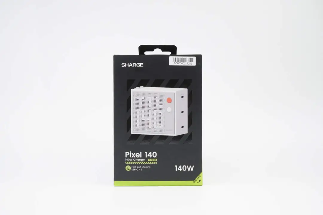
The front of the packaging box is printed with the SHARGE brand, product appearance, Pixel 140W and 140W.
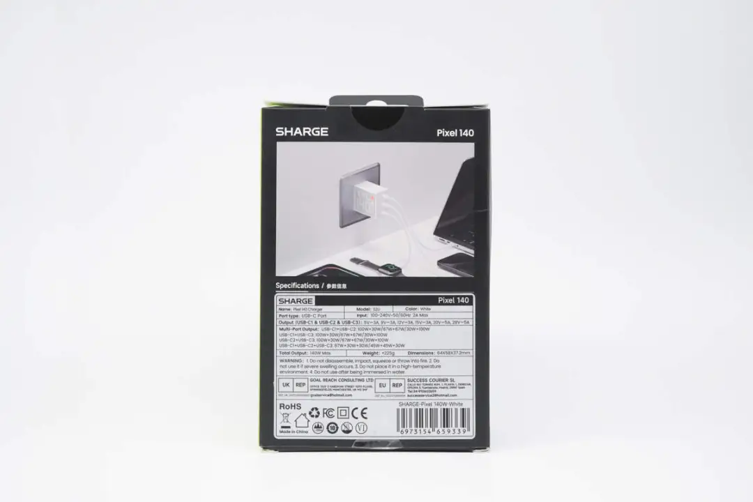
The back of the packaging box is printed with the application scenarios and parameters of the product.
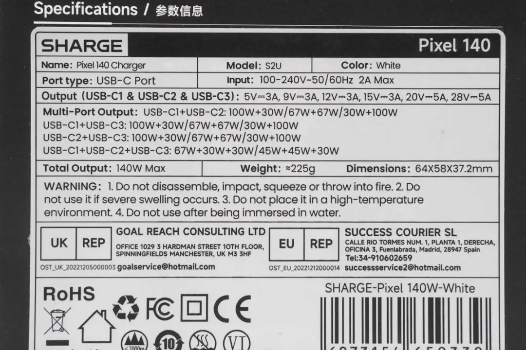
The parameters on the packaging box are close-ups. We will introduce them in detail in the physical product section below.
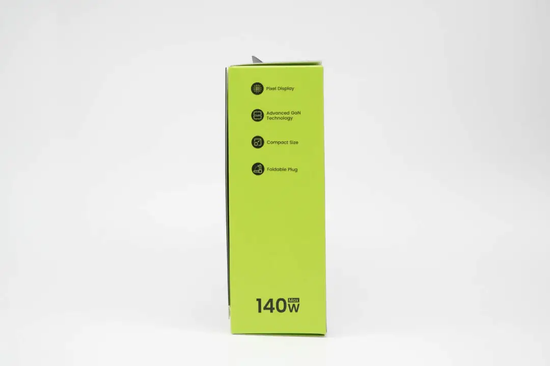
The selling points of the product are marked on the side of the packaging box.
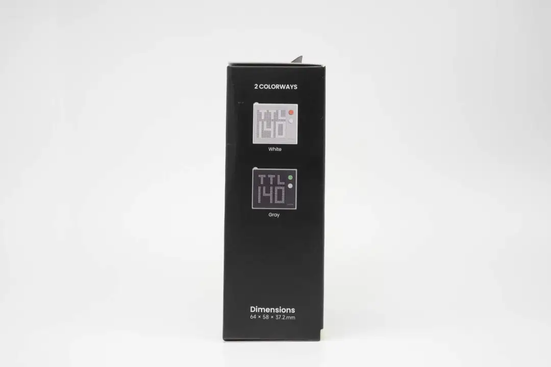
The marking on the other side is available in two colors.
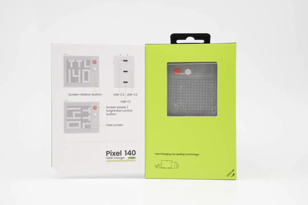
Open the packaging box. The charger is packaged in blister, with instructions for using the buttons printed inside.
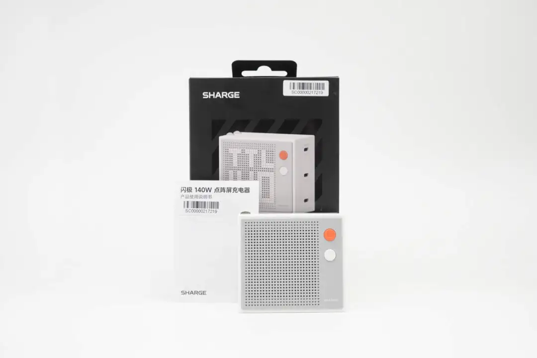
The package contains a 140W gallium nitride charger for the SHARGE Dot matrix screen and an instruction manual.

The side of the SHARGE Dot Matrix screen charger is equipped with a pixel dot matrix digital display.

Below the orange switch button is the white Angle adjustment button. There are corresponding ICONS inside the keys.
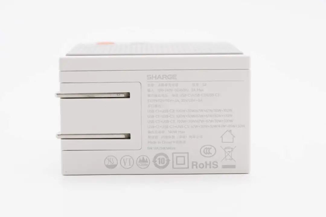
The charger is equipped with folding pins, and the parameters of the charger are printed on the input terminal shell.
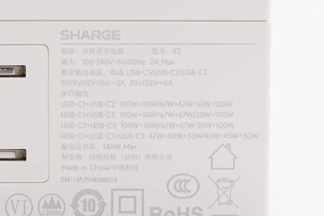
Close-up of Charger Parameters
Name: Dot Matrix Screen Charger
Model: S2
Input: 100-240V~50/60Hz 2A Max
Rated output voltage and current: USB-C1/USB-C2/USB-C3
5V/9V/12V/15V3A, 20/28V5A
Multi-port output
USB-C1+USB-C2:100W+30W/67W+67W/30W+100W
USB-C1+USB-C3:100W+30W/67W+67W/30W+100W
USB-C2+USB-C3:100W+30W/67W+67W/30W+100W
USB-C1+USB-C2+USB-C3:67W+30W+30W/45W+45W+30W
Total output power: 140W Max
Manufacturer: SHARGE (Shenzhen) Co., LTD. The chargers made in China have passed the CCC certification.
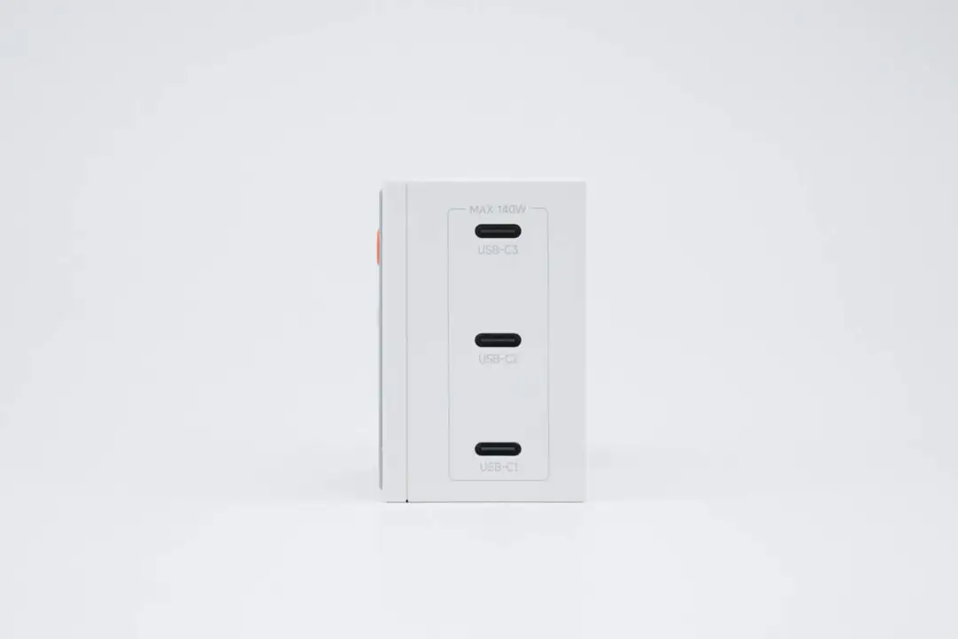
The output terminal of the charger is equipped with three USB-C interfaces.
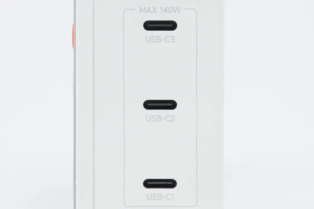
The interface is marked with a maximum output power of 140W.
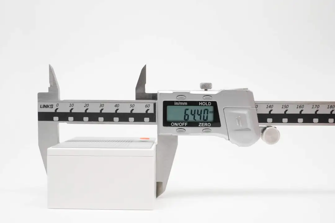
The length of the charger body was measured to be approximately 64.4mm using a vernier caliper.
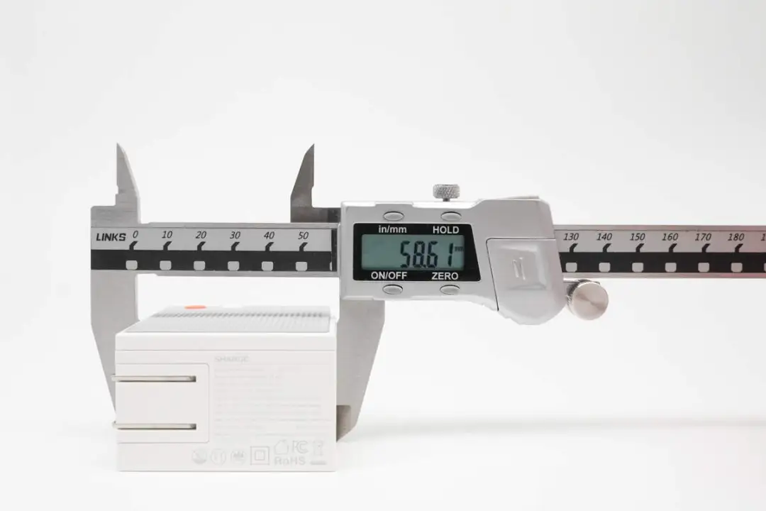
The width of the charger body is approximately 58.6mm.
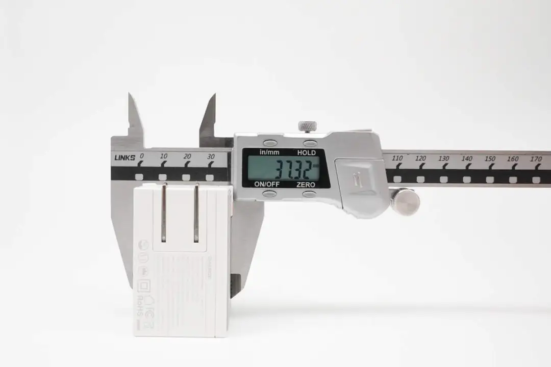
The thickness of the charger body is approximately 37.3mm.
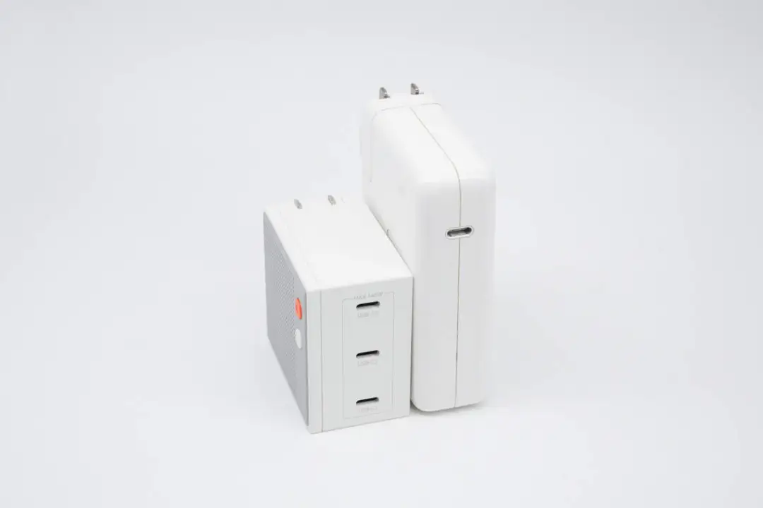
Compared with the 140W charger of Apple, its size has been significantly reduced.
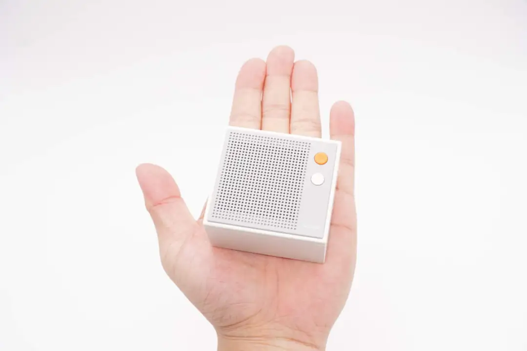
The intuitive perception of the size of the charger when held in hand.
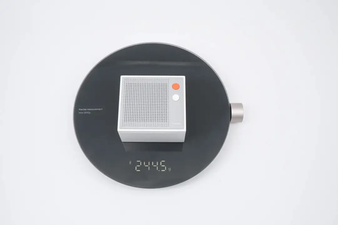
The net weight of the charger was measured to be approximately 244.5g.
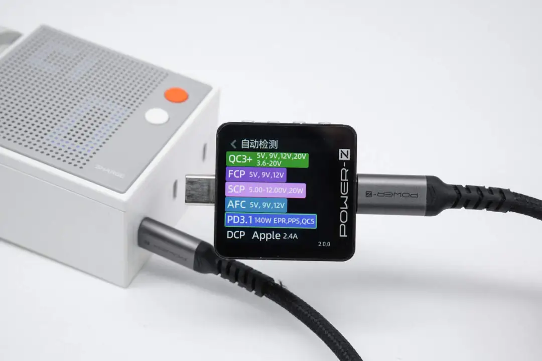
The ChargerLAB POWER-Z KM003C was used to test that the USB-C1/C2/C3 interfaces of the charger support FCP, SCP, AFC, PD3.1, PPS, QC3+/5, DCP, and Apple 2.4A charging protocols.
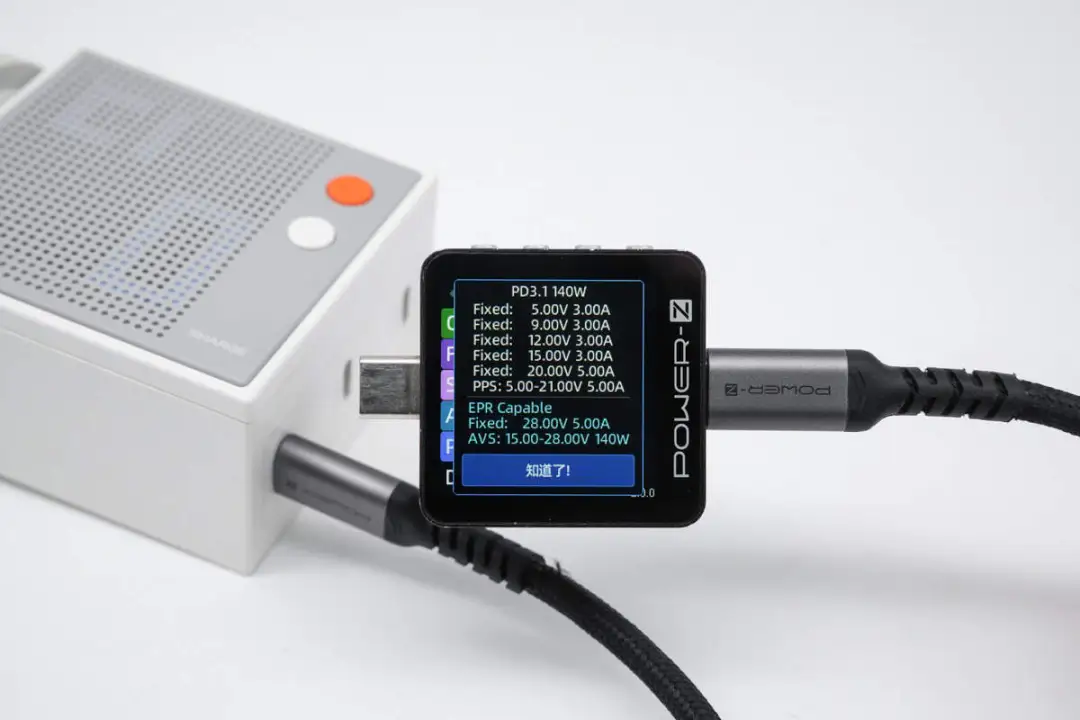
The PDO message shows that the USB-C1/C2/C3 interfaces also have six fixed voltage ranges: 5V3A, 9V3A, 12V3A, 15V3A, 20V5A, and 28V5A, as well as the 5-21V5A PPS voltage range and the 15-28V 140W AVS voltage range.
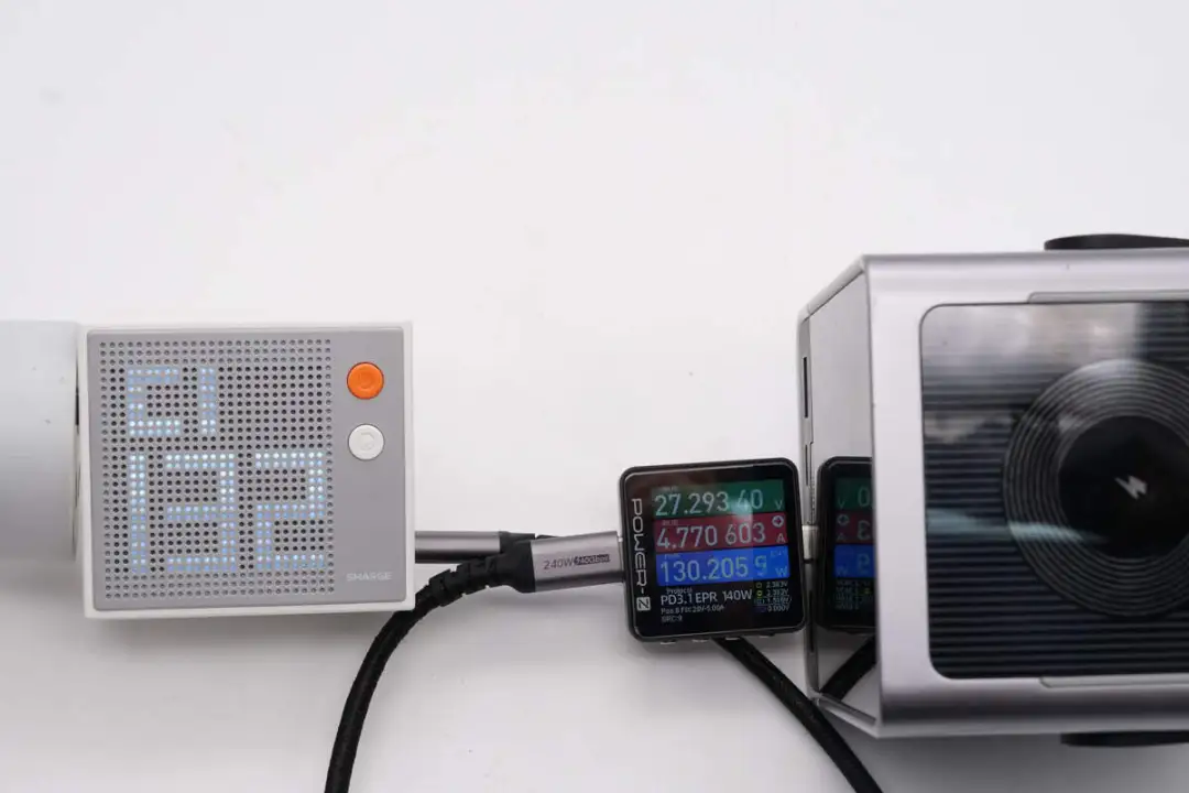
When charging the Cooltech 30 Super Power Warehouse with a charger, the displayed output power is 132W.
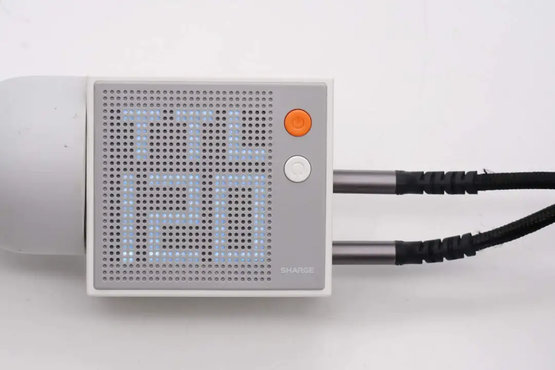
When multiple interfaces of the charger output simultaneously, the total output power is displayed. TTL stands for Total, which means the total output power.
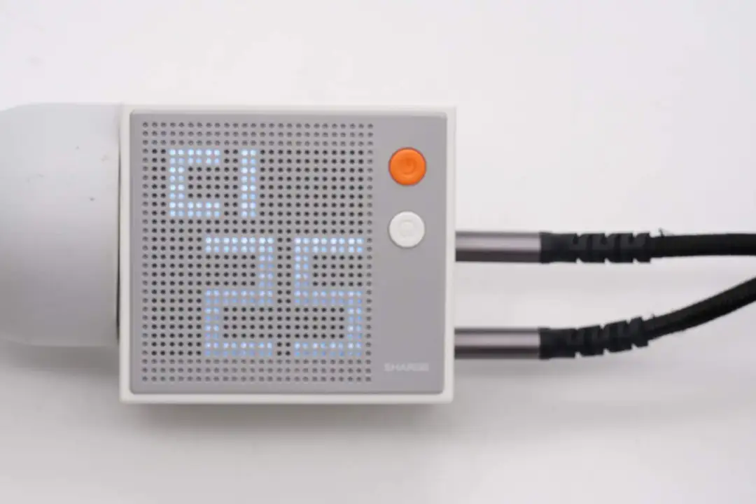
It shows that the output power of the USB-C1 interface is 25W.
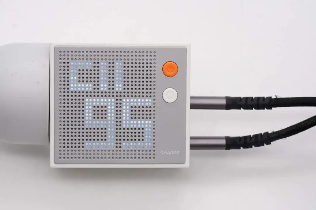
It shows that the output power of the USB-C2 interface is 95W.
Disassembly of 140W Gallium nitride Charger for SHARGE Dot Matrix Screen
After viewing the unboxing demonstration of the SHARGE Dot Matrix Screen gallium nitride charger, let's now disassemble it and take a look at the internal design and materials together.
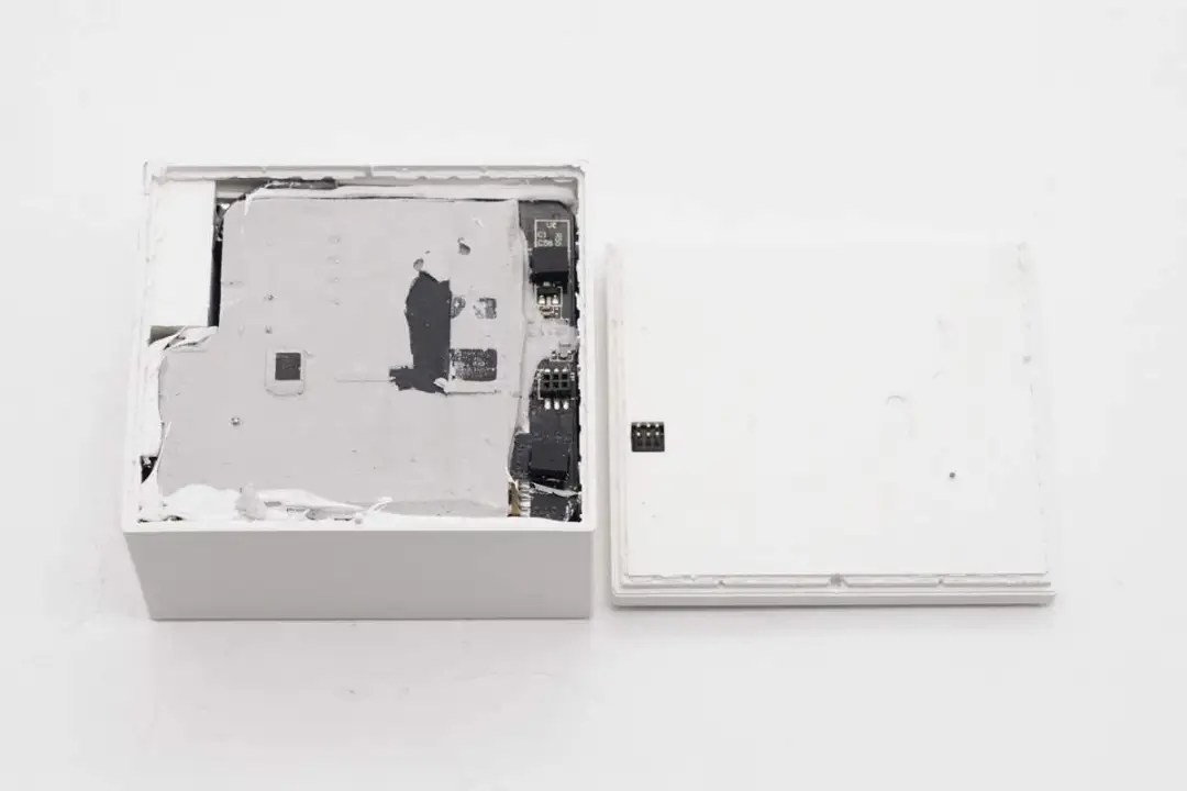
Pry open the dot matrix screen module along the joint of the shell, and the shell is fixed by ultrasonic welding.
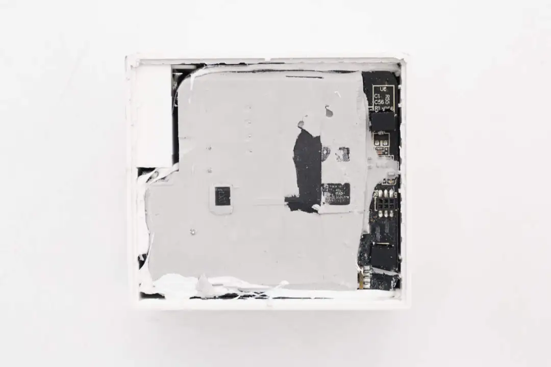
The internal PCBA module is filled with glue to enhance heat dissipation performance and weather resistance.
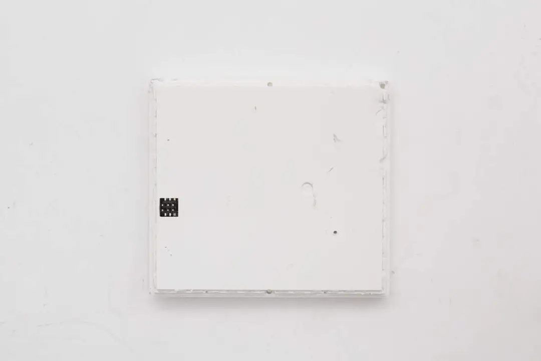
The dot matrix screen module is connected to the charger PCBA module through pin headers.
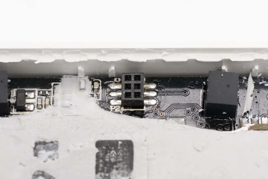
The PCBA module is equipped with connection sockets.
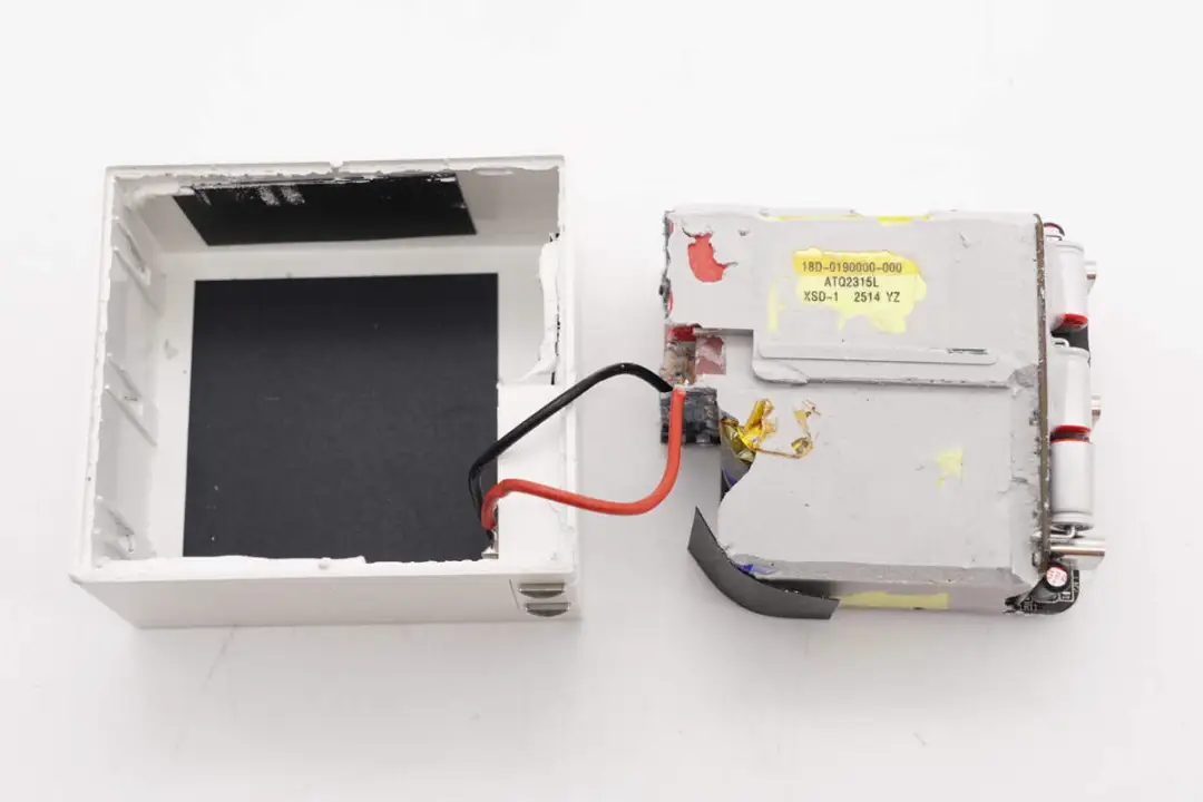
The folding pins are connected to the PCBA module through wires, and graphite thermal conductive stickers are pasted inside the shell.
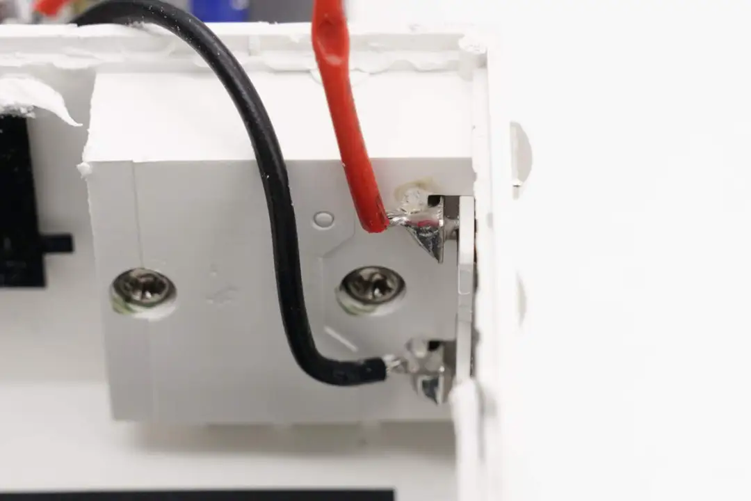
The wires are welded to the folding pins.
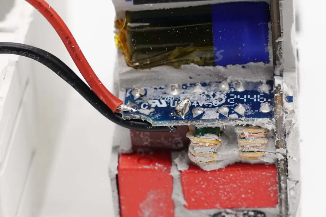
The other end is welded to the PCBA module.
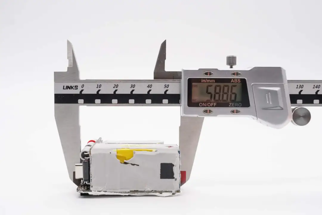
The length of the PCBA module was measured to be approximately 58.9mm using a vernier caliper.
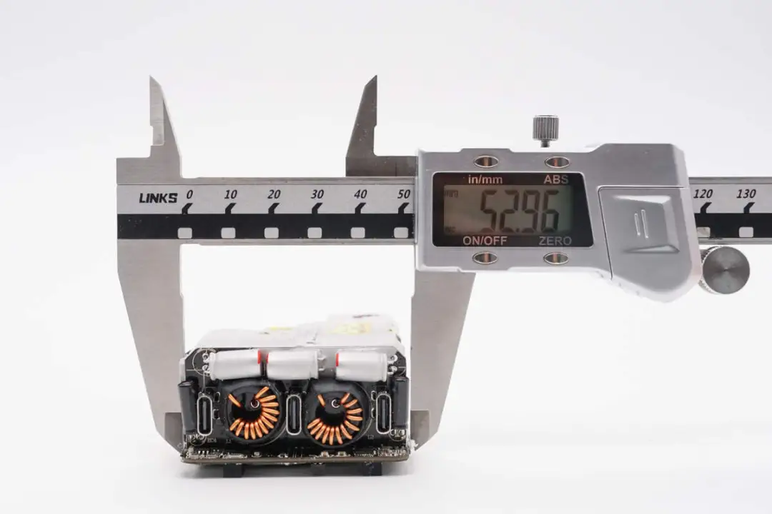
The width of the PCBA module is approximately 53mm.
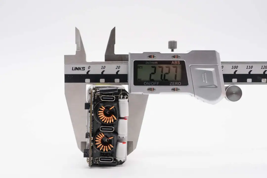
The thickness of the PCBA module is approximately 27.3mm.
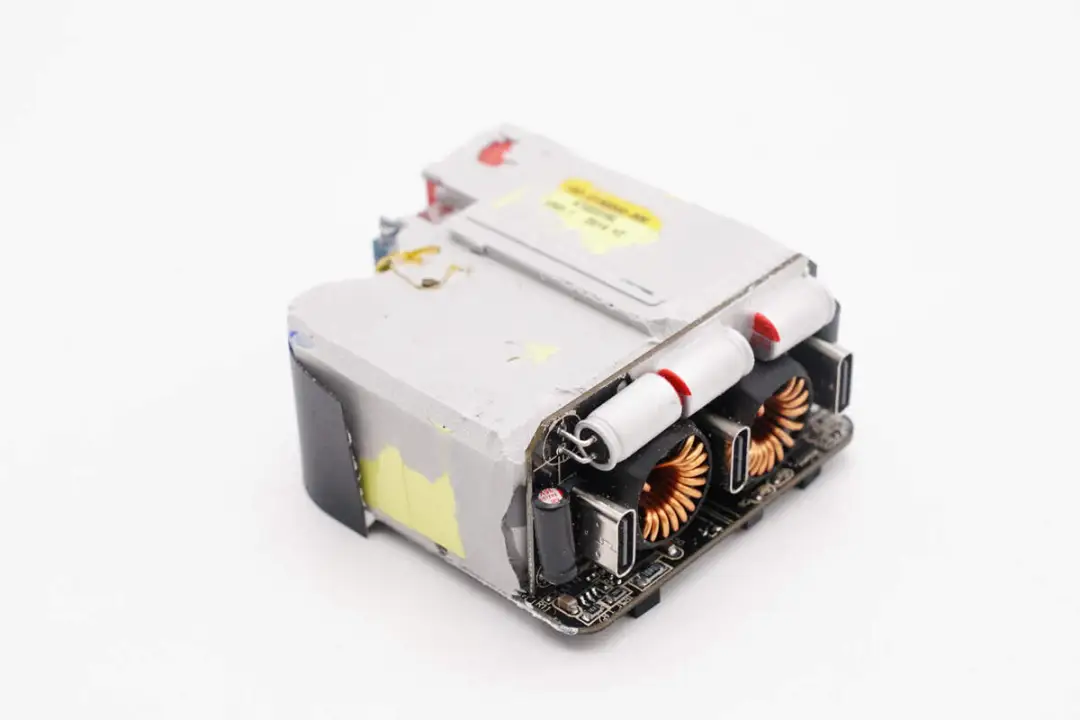
The PCBA module is composed of multiple small boards welded together.
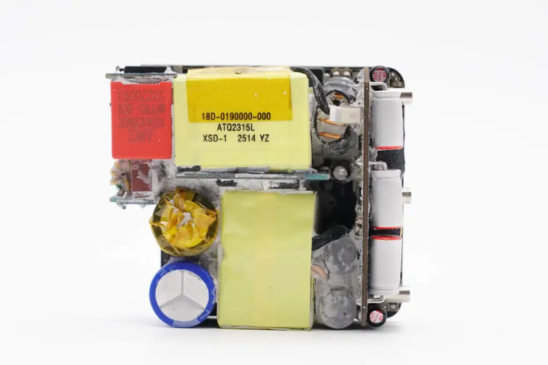
Remove the thermal conductive adhesive. A view of the front of the PCBA module: on the left is the input end, where the fuse small board and the rectifier bridge small board are welded. Above is the PFC small board. Below are the high-voltage filter capacitor and the transformer. The output filter capacitor is insulated with a silicone sleeve. On the right is the voltage-reducing output small board.
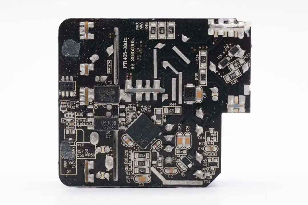
The back of the PCBA module is equipped with an AHB gallium nitride encapsulated chip, a surface mount Y capacitor, and a feedback optocoupler.
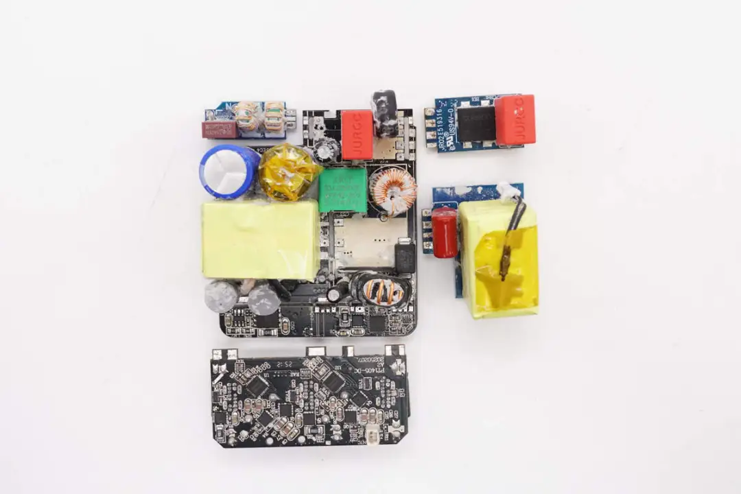
Weld and disassemble each small board, and continue the disassembly process. Through the observation of the PCBA module, it was found that the 140W gallium nitride charger of the SHARGE Dot Matrix screen adopts a PFC+AHB architecture design, and the output uses a three-channel synchronous step-down chip output. Among them, the PFC switch tube is from Nanomicro, and the AHB uses Dongke gallium nitride encapsulated chips.
The AHB architecture enhances the conversion efficiency by recovering and utilizing the leakage inductance energy in traditional flybacks, while maintaining the wide-range voltage output advantage of the flyback architecture. Dongke's AHB gallium nitride integrated chip has a high degree of integration and is highly suitable for single-port high-power PD fast charging applications. For fixed-voltage output scenarios in multi-port fast charging, its conversion efficiency can be comparable to that of LLC, and it also has a cost advantage.
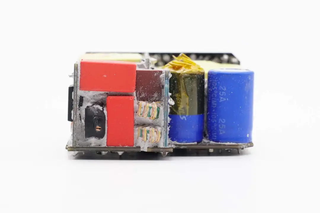
Two small boards are welded to the input end of the charger to form an EMI circuit, which improves space utilization and reduces volume. The high-voltage filter capacitor on the right side is wrapped with high-temperature tape for insulation.

The front of the input small board is soldered with a fuse and two common mode inductors.
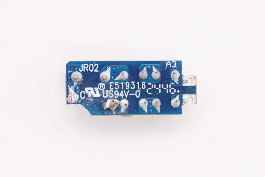
There are no components on the back of the small board.
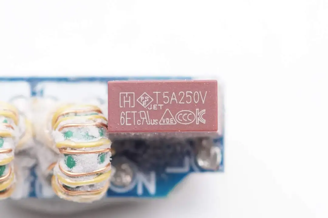
The fuse specification at the input end is 5A 250V.
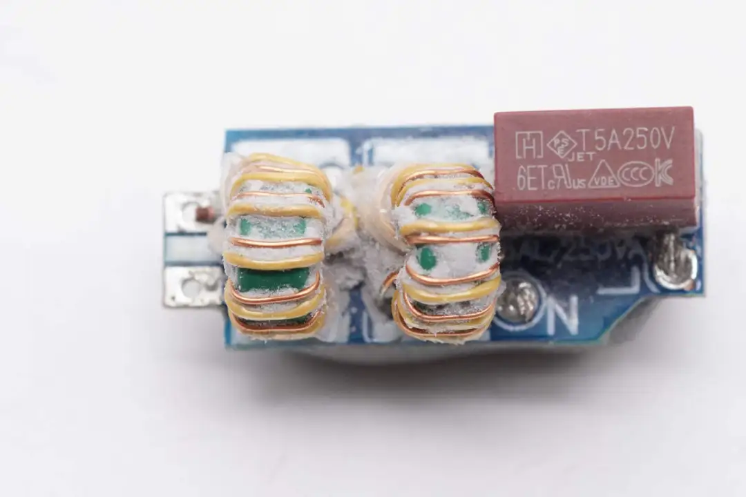
Common mode inductors are wound with enameled wire and insulated wire.
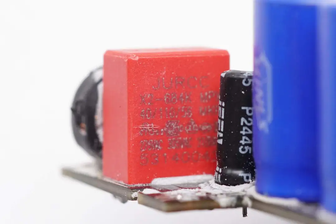
The safety standard X2 capacitor is from Jiewei Electronics and has a capacity of 0.68μF.
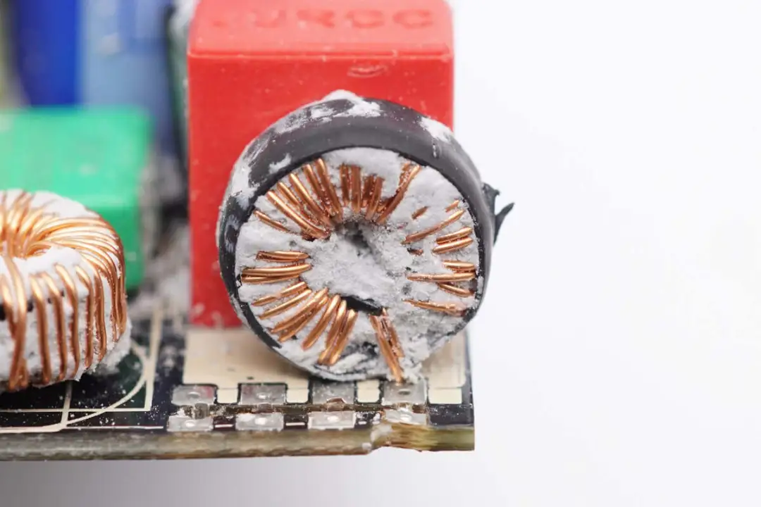
The filter inductor adopts magnetic winding system and is insulated by heat shrink tubing on the outside.
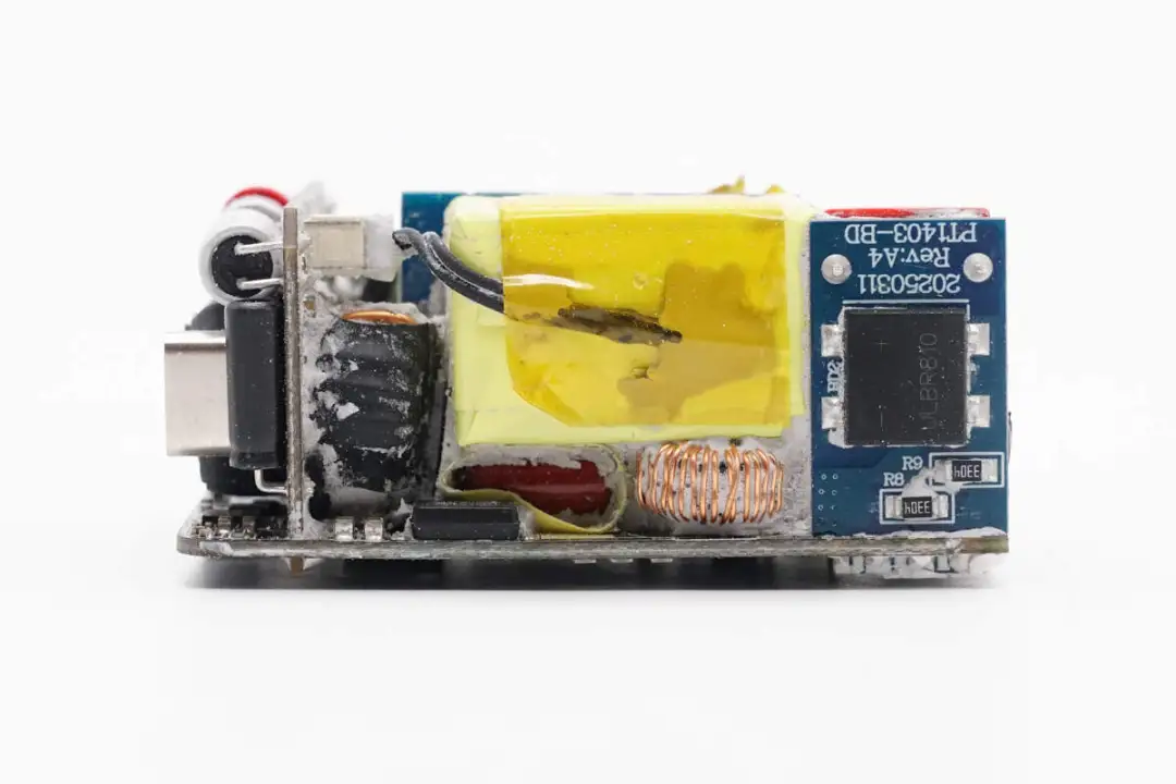
The PFC inductor on the side is pasted with a thermistor for temperature detection. Below it, there are film filter capacitors and filter inductors. On the right side, a small plate is welded with a rectifier bridge.
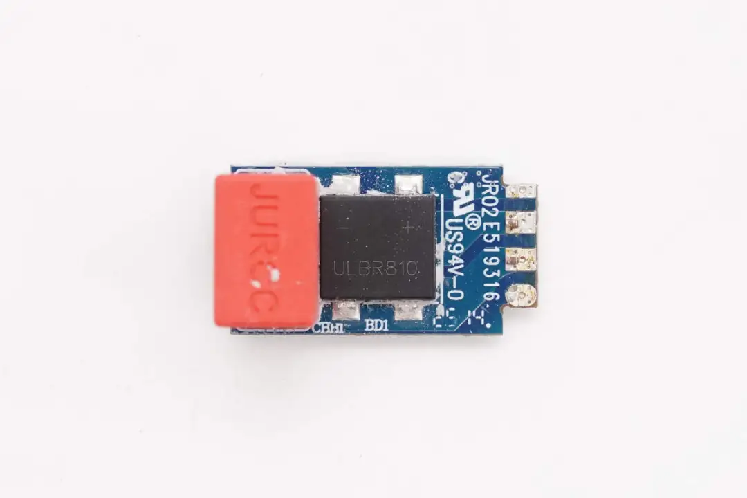
Another small plate is welded with a rectifier bridge and a film filter capacitor.
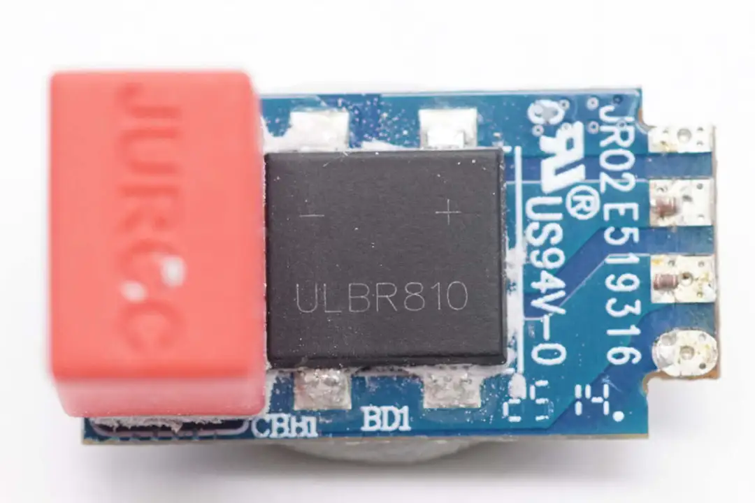
Rectifier bridge silk-screened ULBR810, specification 8A 1000V.
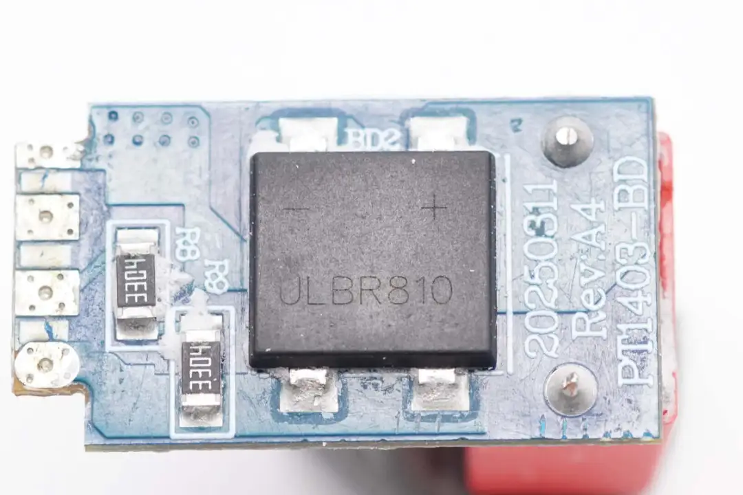
A rectifier bridge of the same model is welded to the back of the small plate. The rectifier bridge is connected in half Bridges to evenly distribute the heat and reduce the temperature rise.
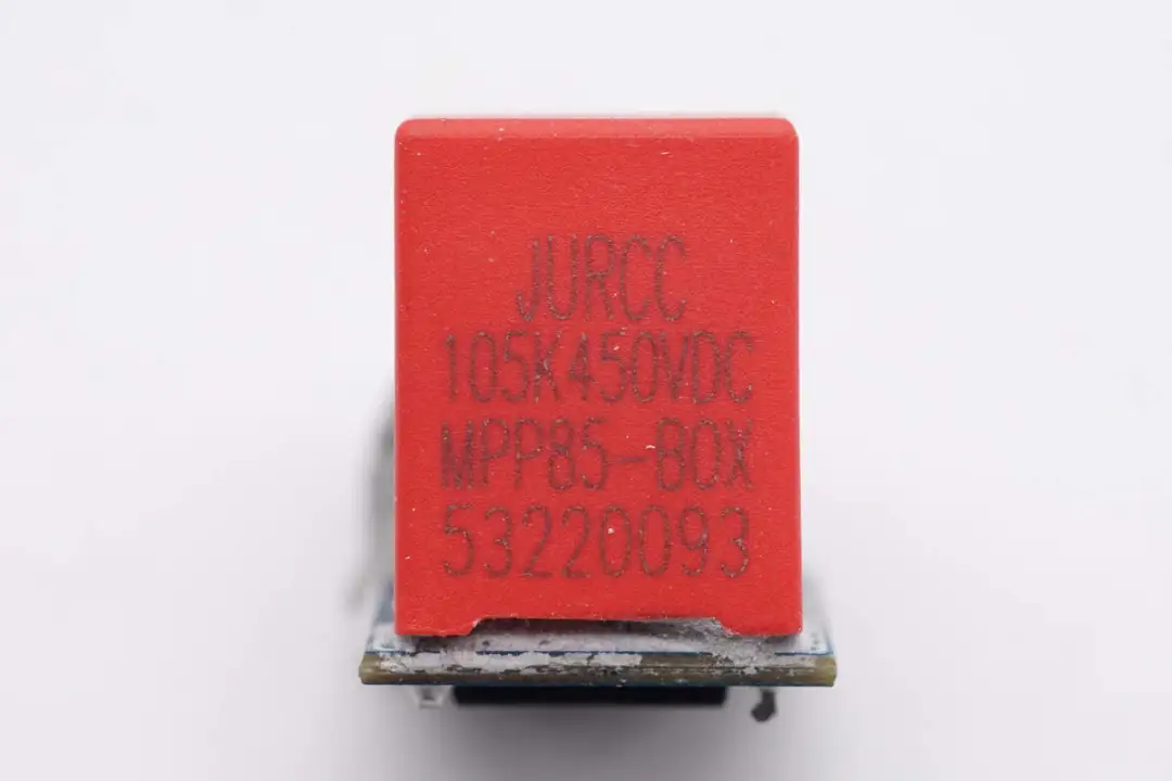
The film filter capacitor is from Jiewei Electronics, with a specification of 1μF450V.
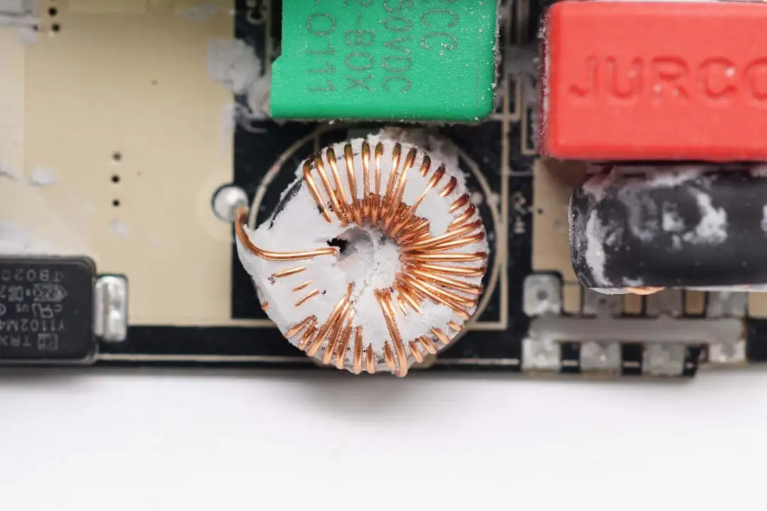
A close-up of the filter inductor soldered below the PFC inductor.
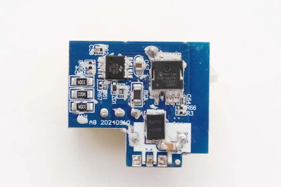
PFC small board welding PFC controller, PFC switch tube and PFC rectifier tube.
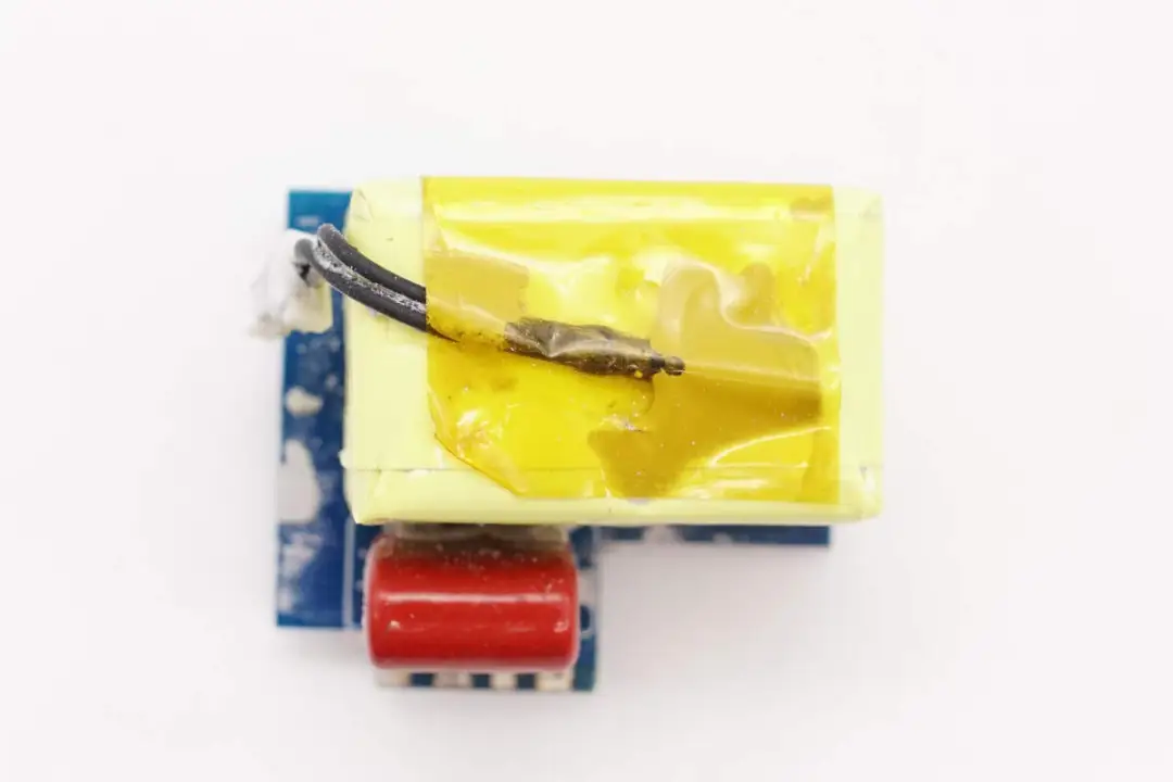
On the other side, solder the boost inductor and the film filter capacitor.
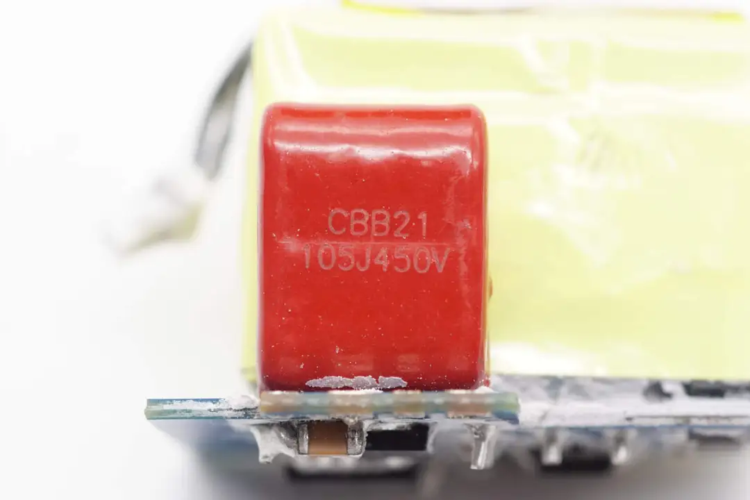
The specification of the film filter capacitor is 1μF450V.
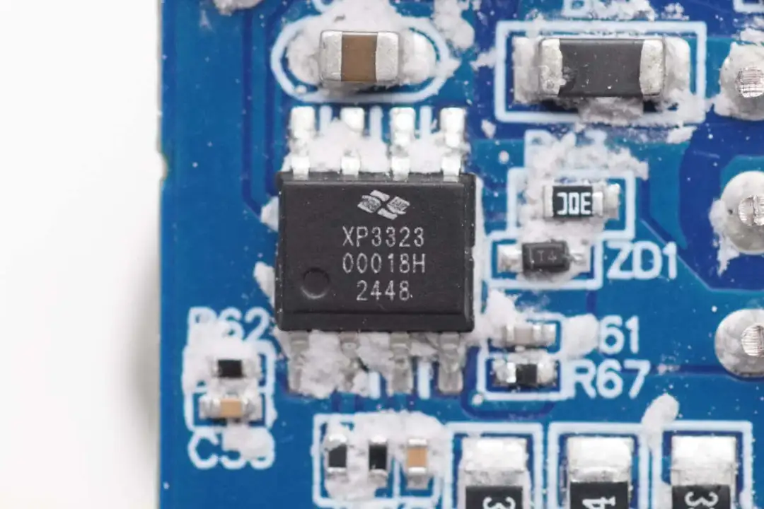
The PFC controller is from Xinguo, model XP3323. It is a borderline mode PFC controller. The chip adopts a patented digital power control algorithm, featuring excellent dynamic performance and light-load PF/THD performance. It is packaged in SOP8.
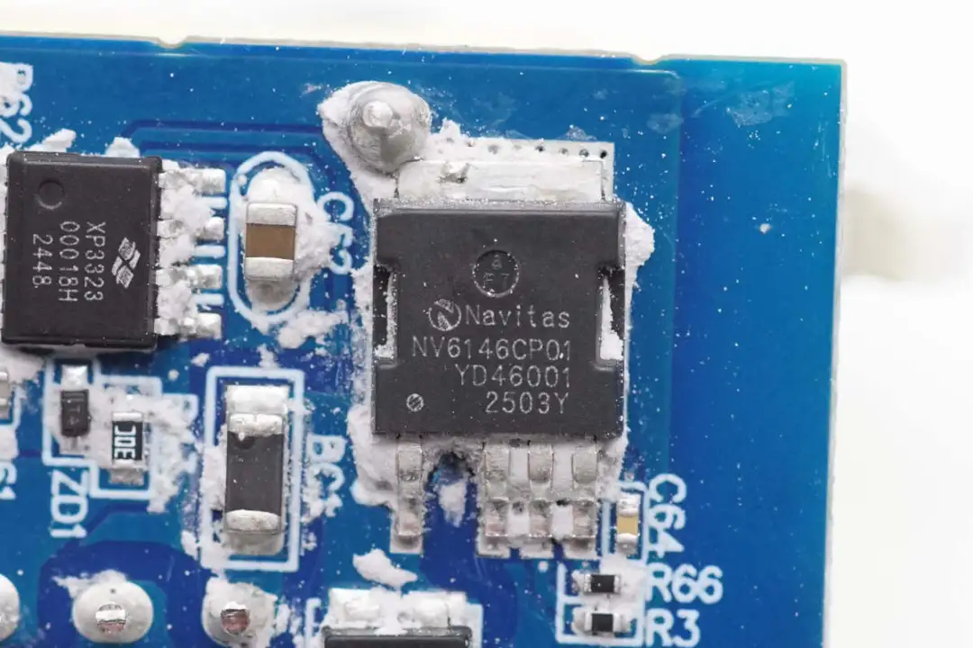
The PFC switch tube is from Navitas, model NV6146C, which is a Navitas GaNSlim gallium nitride power chip. The chip integrates a high-performance enhanced gallium nitride device with a 700V withstand voltage and a 170mΩ resistance. It integrates a gate driver and lossless current sampling, and supports overheat protection. It is suitable for fast charging, wireless power transmission, and LED lighting. Solar micro-inverters, server power supply and other applications adopt the DPAK-4L package.
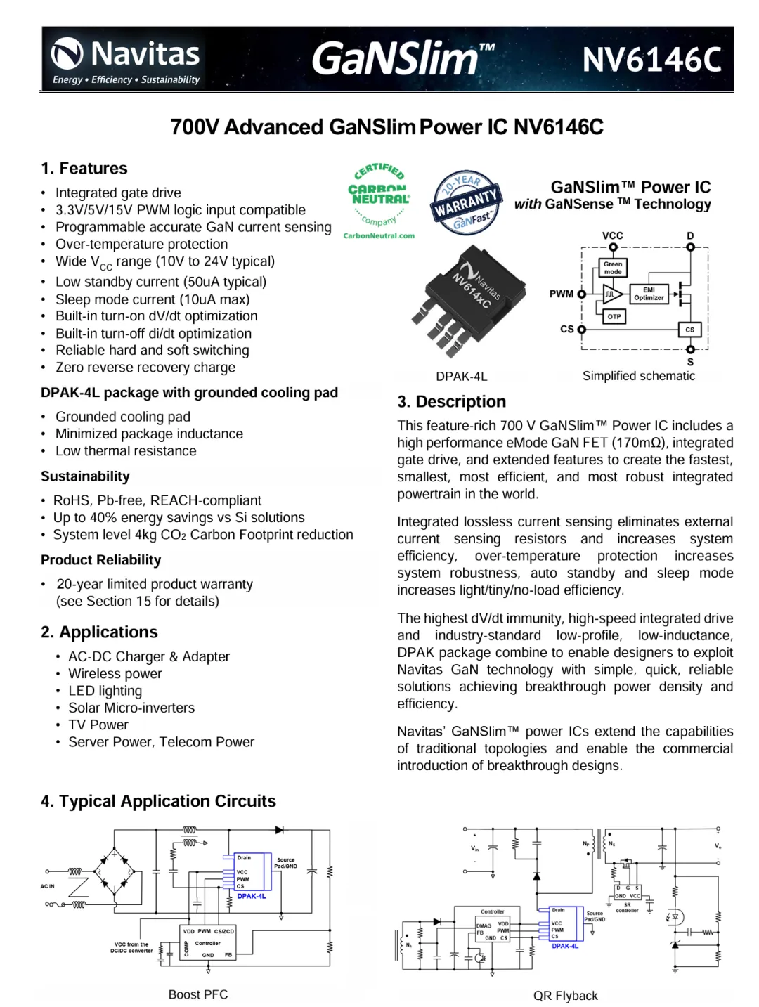
Data information of Nanomicro NV6146C.
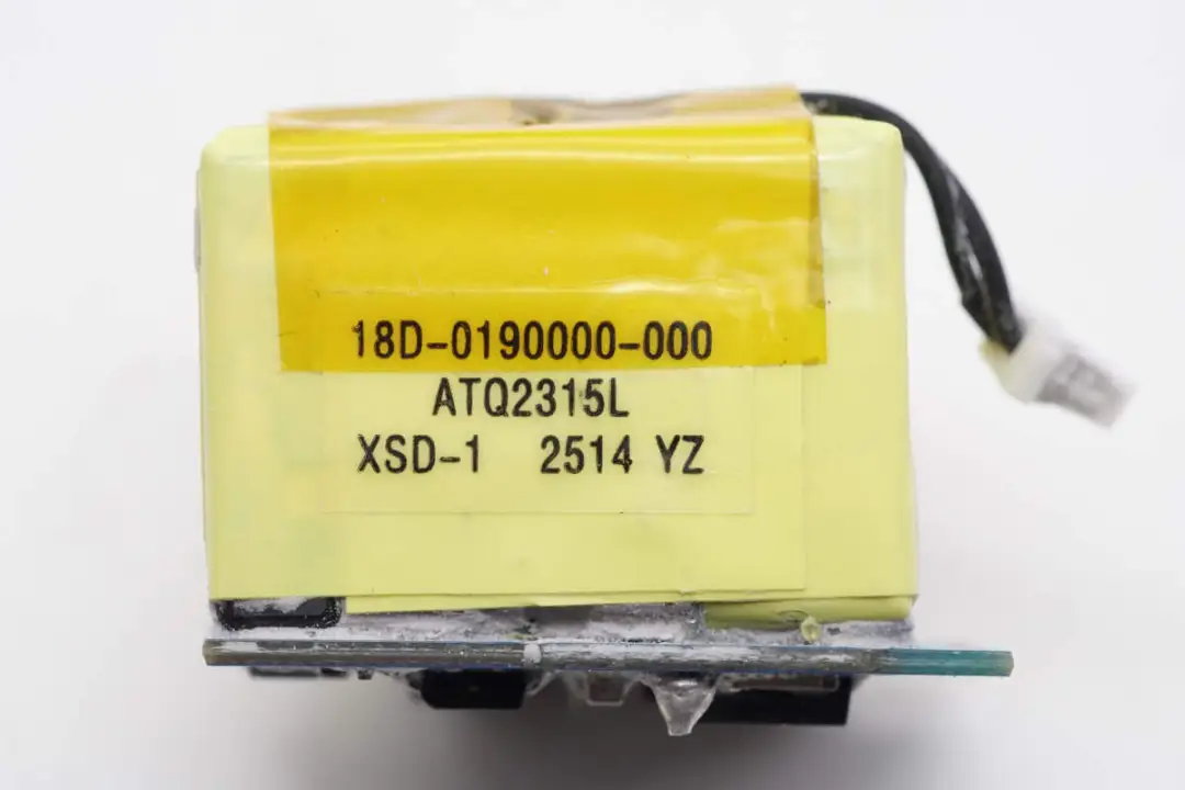
The PFC boost inductor is wound with ATQ2315L magnetic core.
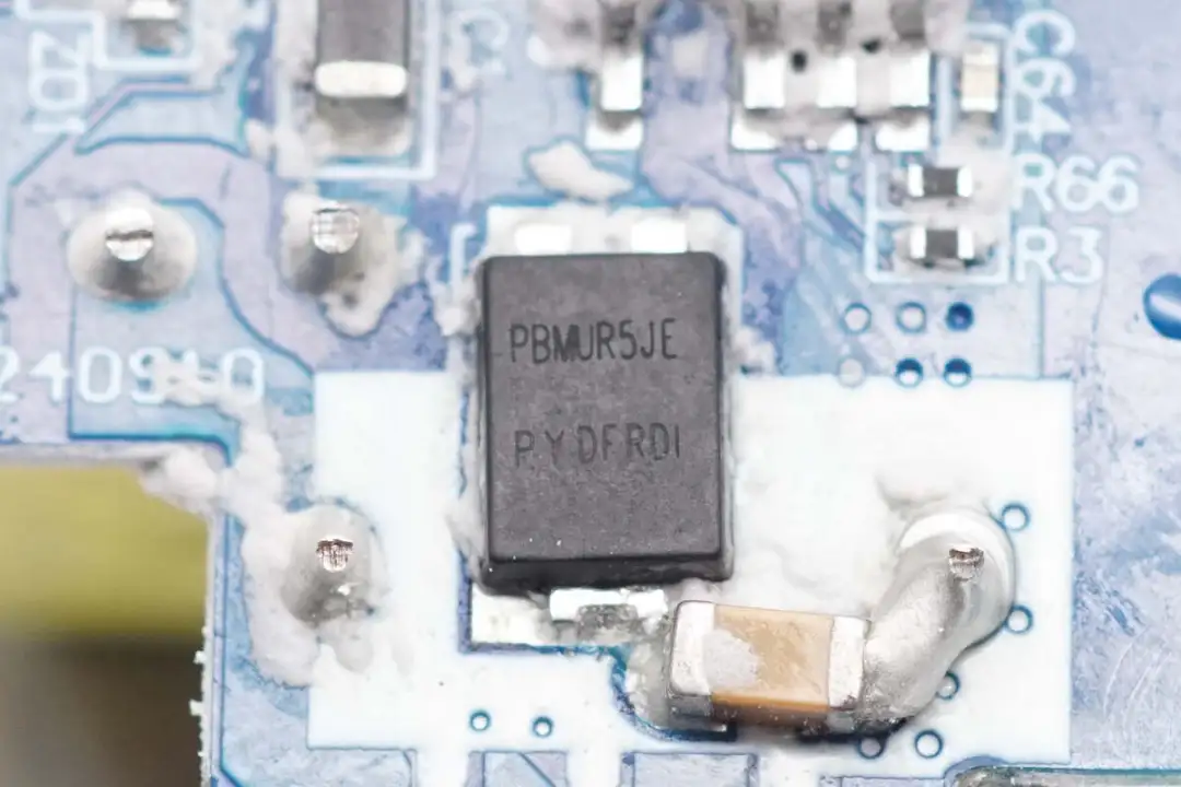
The PFC rectifier tube is from Pingwei, model PBMUR5JE. It is an ultra-fast recovery diode with a specification of 600V 5A and is packaged in PS-277B.
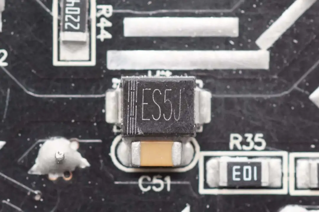
The ES5J diode is used for PFC bypass.
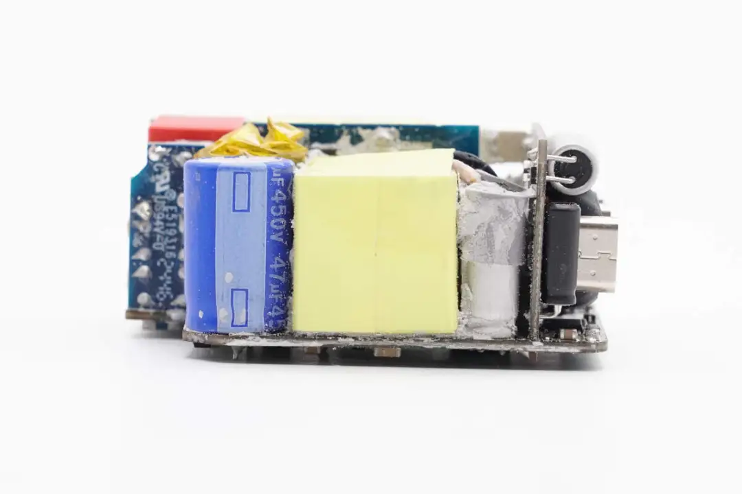
A side view of the PCBA module shows that it is equipped with high-voltage filter capacitors, transformers, solid-state filter capacitors and output small boards.
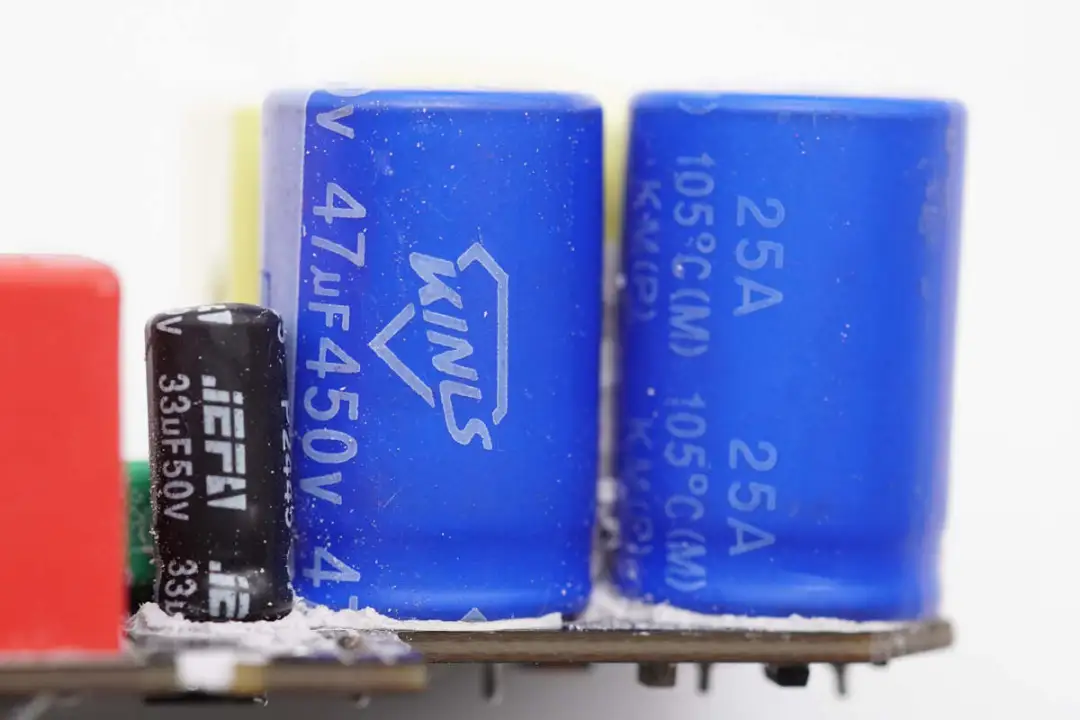
The high-voltage filter capacitor is from sapphire, with a specification of 47μF450V.
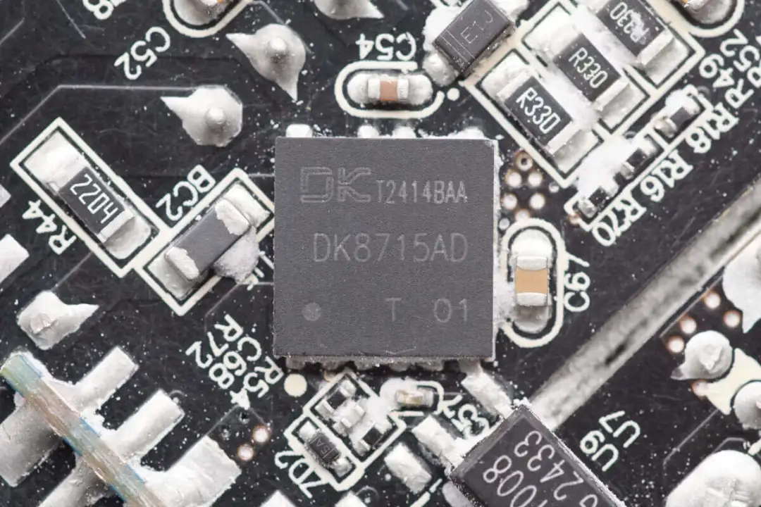
The AHB gallium nitride integrated chip is from Dongke Semiconductor, model DK8715AD. It is an AC-DC power switch chip based on an asymmetric half-bridge architecture, integrating two gallium nitride power devices. It can achieve the primary power transistor ZVS and the secondary rectifier transistor ZCS within a wide load range, thereby improving the efficiency of the power supply system. At the same time, soft switching can also reduce the stress of power transistors and has a built-in full-range frequency jitter circuit, thereby reducing switching losses and improving electromagnetic interference.
The DK8715AD supports a maximum switching frequency of 800KHz. When the front end is equipped with a boost PFC, the recommended power is 150W, and the standby power consumption is less than 50mW. It features adaptive dead zone and turn-off algorithms, eliminating the need for peripheral adjustment and minimizing the peripheral design. It also has halogen-free characteristics and complies with ROHs requirements. Additionally, it is built-in with high-voltage start and X capacitor discharge circuits. Provide higher performance and reliability for the system. The DK8715AD ADAPTS to four load modes, effectively enhancing the efficiency of each load segment. By installing the DK8715AD, the conversion efficiency can reach up to 95.4% at most.
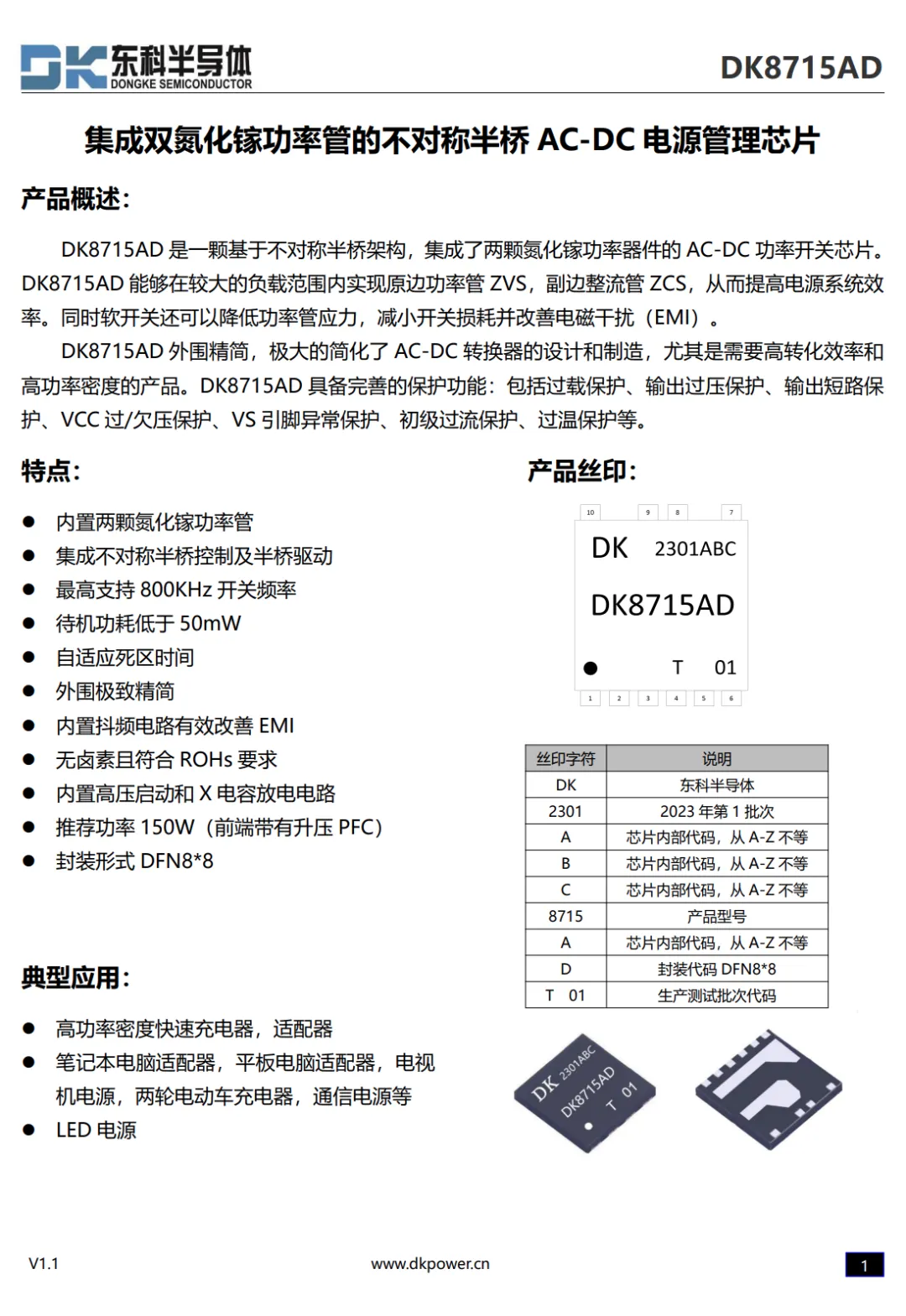
The DK8715AD is equipped with two 650V enhanced GaN HEMTs, featuring an integrated half-bridge drive circuit and an asymmetric half-bridge control circuit. The upper and lower tubes can adapt to the dead time and turn-off algorithm. Among them, the lower tube (main power tube) ADAPTS to the dead time, and the upper tube (resonant tube) ADAPTS to the turn-off time. There is no need for external adjustment, which greatly simplifies the scheme design and debugging. It is also equipped with multi-functional pins, which can be used for demagnetization detection, output OVP, Brown in/out and other functions. It also has the CS negative pressure sampling function to improve the driving stability.
The DK8715AD has a streamlined periphery, which can greatly simplify the design and manufacture of AC-DC converters, especially for products that require high conversion efficiency and high power density. The DK8715AD is equipped with comprehensive protection functions, including overload protection, output overvoltage protection, output short circuit protection, VCC overvoltage/undervoltage protection, VS pin anomaly protection, primary overcurrent protection, over-temperature protection, etc.
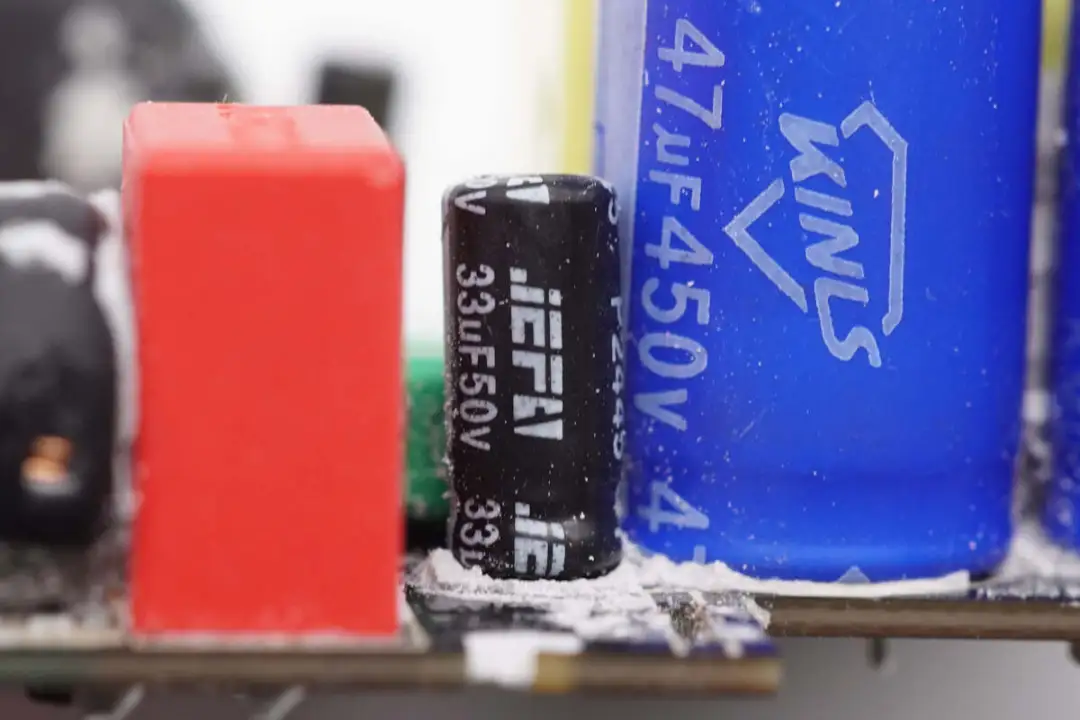
The filter capacitor that powers the main control chip is from Jiefa, with a specification of 33μF50V.
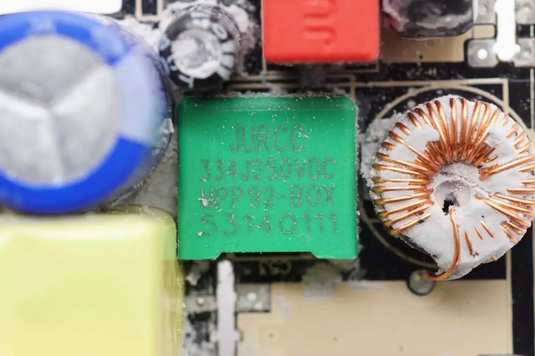
The resonant capacitor is from Jiewei Electronics, with a specification of 0.33μF to 250V.
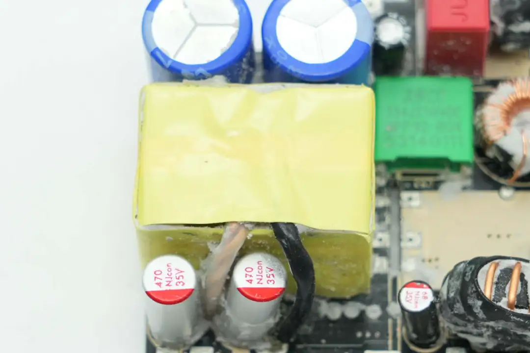
The transformer is insulated by tightly winding adhesive tape.
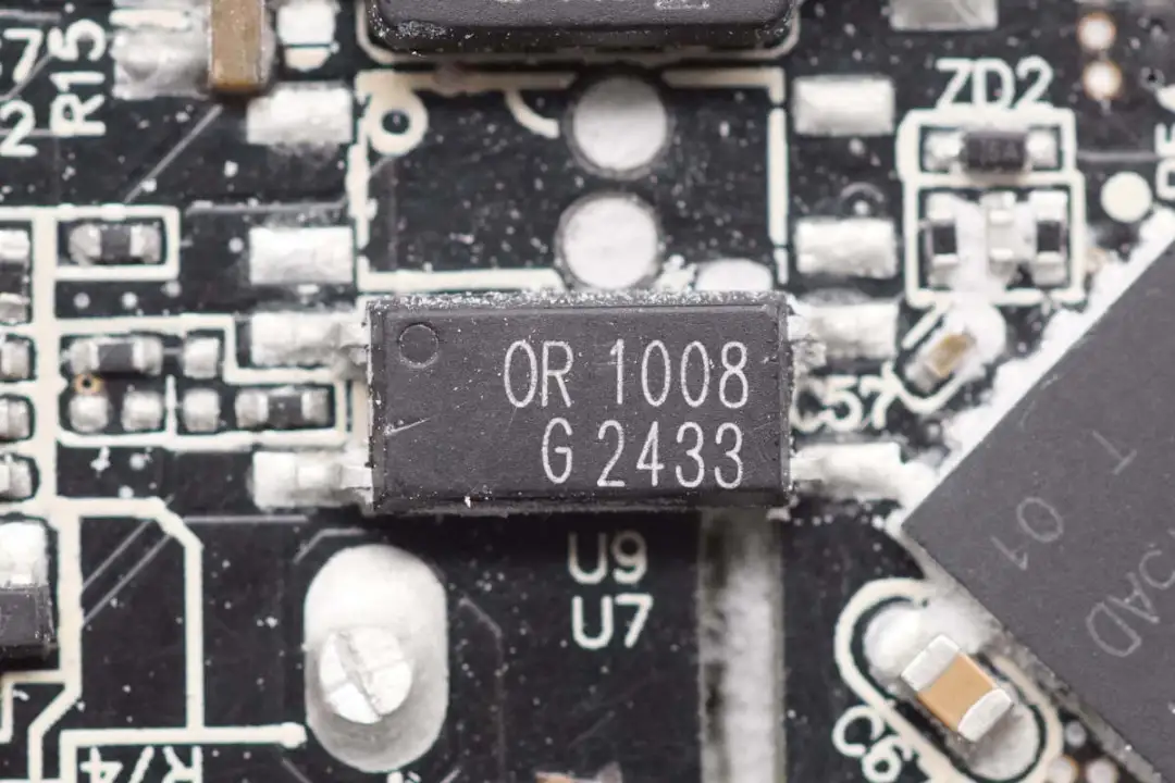
The ORlund OR1008 optocoupler is used for output voltage feedback regulation.
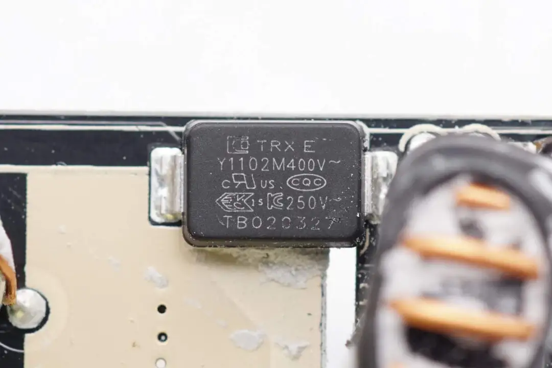
The surface mount Y capacitors are from Sichuan Terui Xiang Technology Co., LTD. They feature small size and light weight, making them highly suitable for application in high-density power supply products such as gallium nitride fast charging. The material number is TMY1102M.
Charging Head Network has learned that In addition to being used in dozens of high-power chargers such as the 100W gallium nitride fast charger certified by Bex Qualcomm QC5, the 100W gallium nitride charger from Meiduoduo, the 65W Super SHARGE Charge gallium nitride charger from OPPO, the 90W gallium nitride fast charger from Lenovo, the 65W gallium nitride charger from Nubia, and the 120W gallium nitride + silicon carbide PD fast charger from Bex It can also be applied to 20W mini fast charging devices of brands such as Hailutong, First Guard, and Belkin, and its performance has been unanimously recognized by customers.
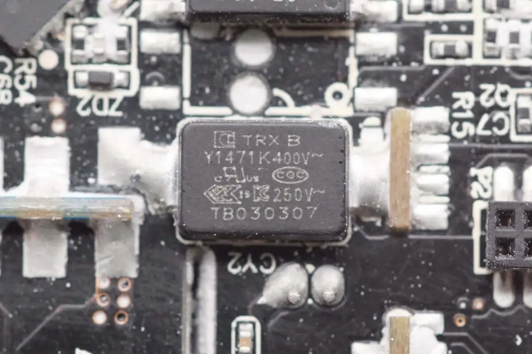
Another piece has the material number TMY1471K.
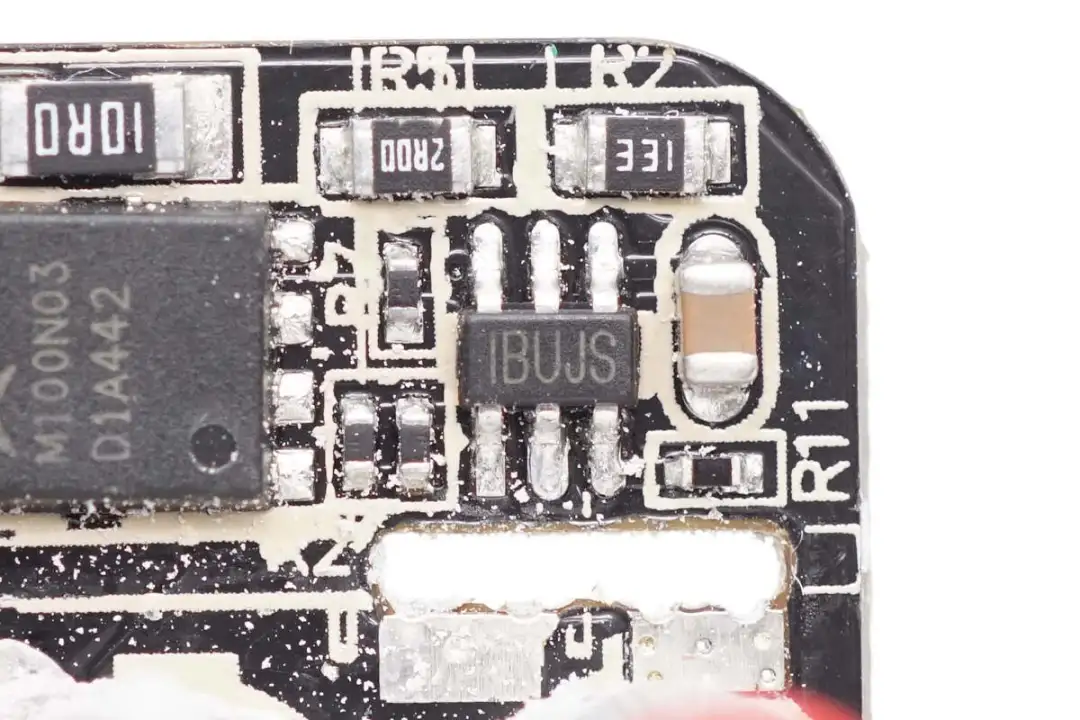
The synchronous rectifier controller from Xinyuan System, with a silk-screen printing of BUJ and model MP6951, is the latest synchronous rectifier controller launched by Xinyuan System. It supports DCM, CCM, QR, and ZVS working modes, and also supports ACF active clamping flyback and HFB hybrid flyback. The working frequency can reach 1MHz, and it supports driving gallium nitride synchronous rectifier tubes. Supports high-side and low-side applications and is packaged in TSOT23-6.
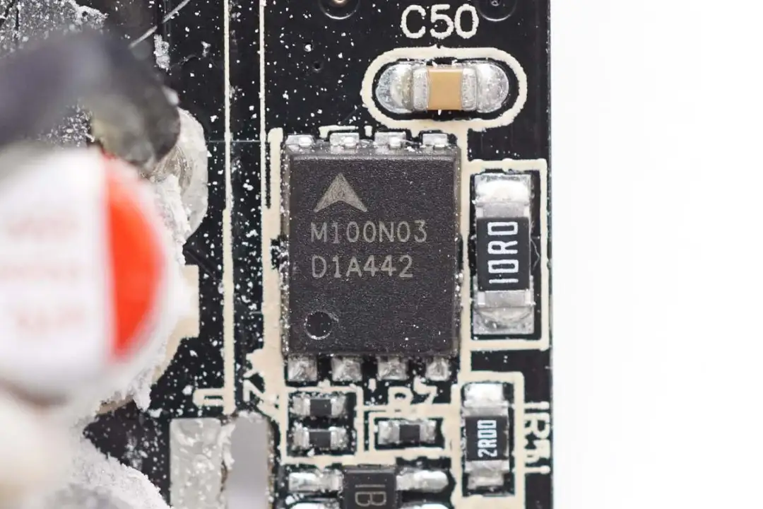
Synchronous rectifier tube silk-screened M100N03, in DFN5*6 package.
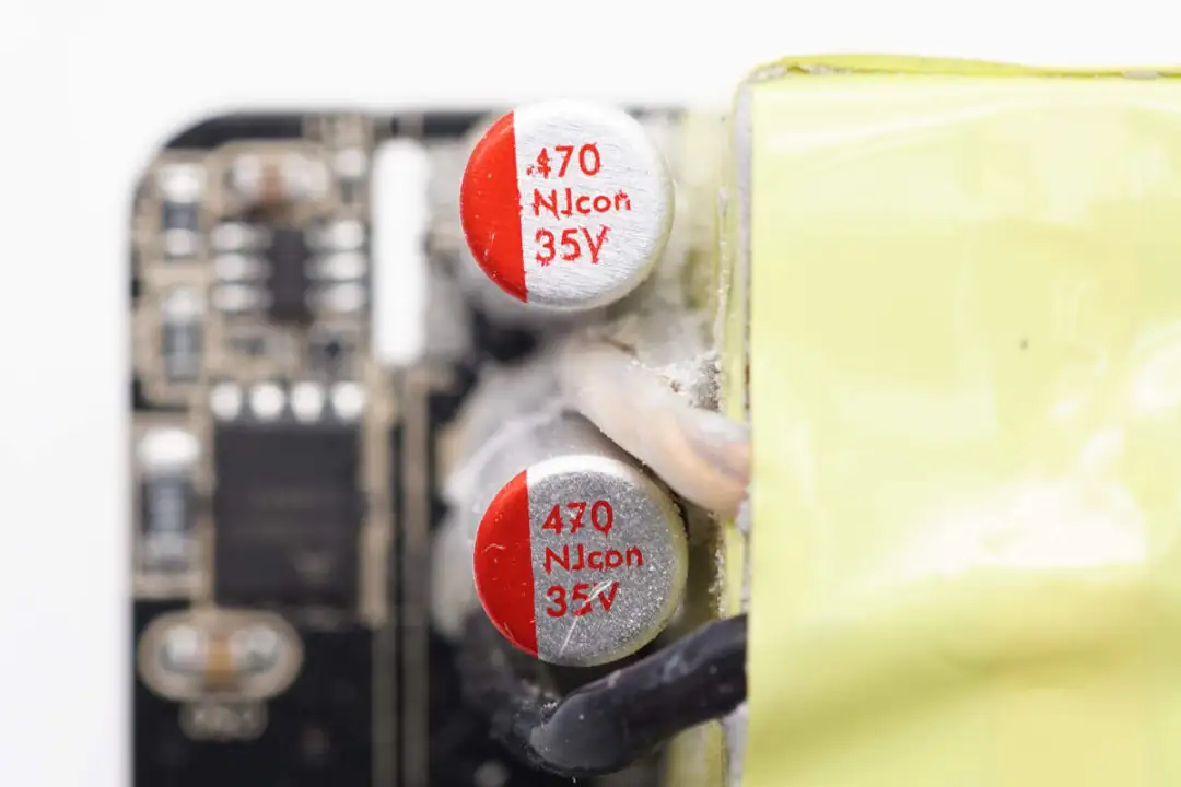
The filter solid-state capacitors are from Yongli, with a specification of 470μF35V, and two are connected in parallel.
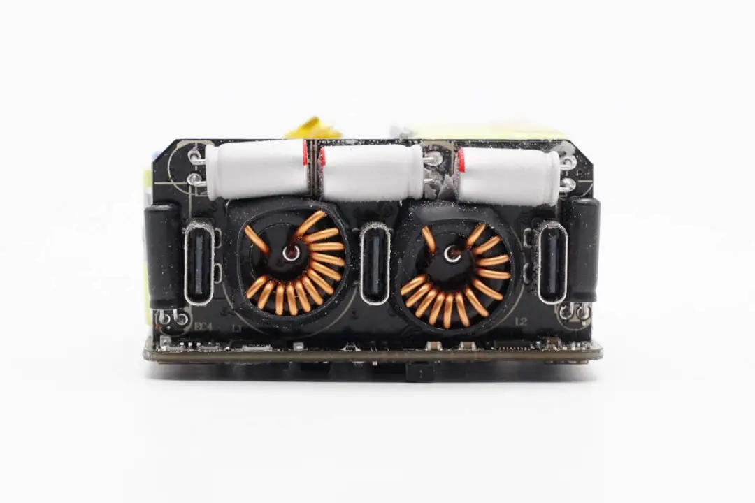
A vertical small plate is welded to the output end of the charger.
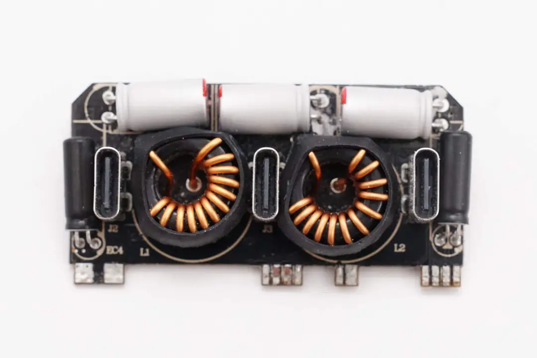
Solder the USB-C interface, magnetic ring step-down inductor and filter capacitor on the small board.
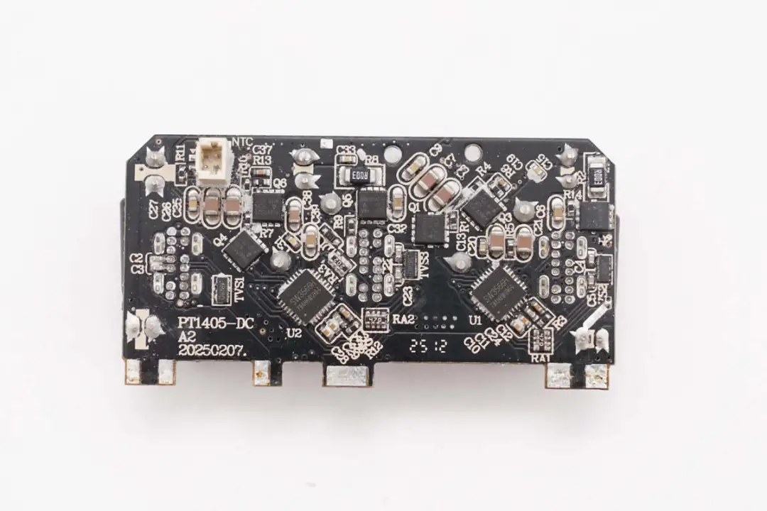
The back of the small board is welded with a step-down protocol chip, along with the corresponding synchronous step-down tube and VBUS switch tube. The USB-C female socket is via welding, which is firm and durable.
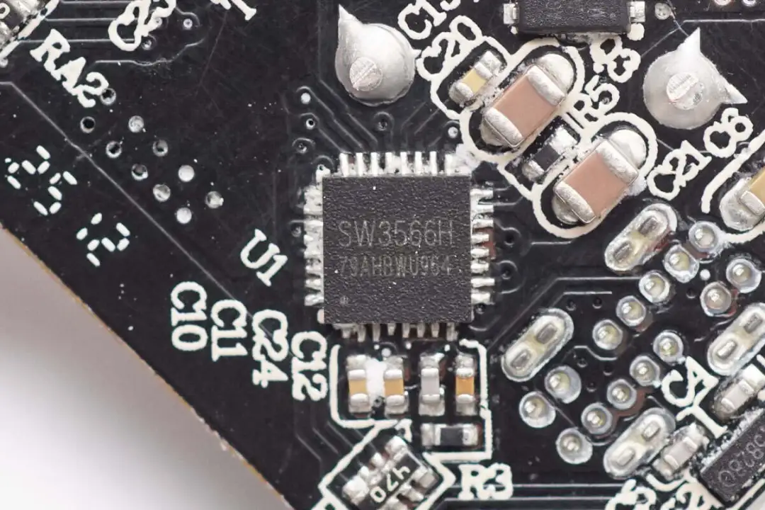
The USB-C1 interface of the charger uses the Zhirong SW3566H step-down protocol chip. This chip is a highly integrated multi-fast charging protocol dual-port charging SOC chip, supporting USB-C and USB-A interface charging, and supporting independent current limiting for both ports. The chip integrates a high-efficiency synchronous step-down converter internally, supporting 20V7A and 28V5A outputs. It supports fast charging protocols such as PD3.1/QC/SCP/UFCS, and allows for customized fast charging protocols, with a maximum output power of 140W.
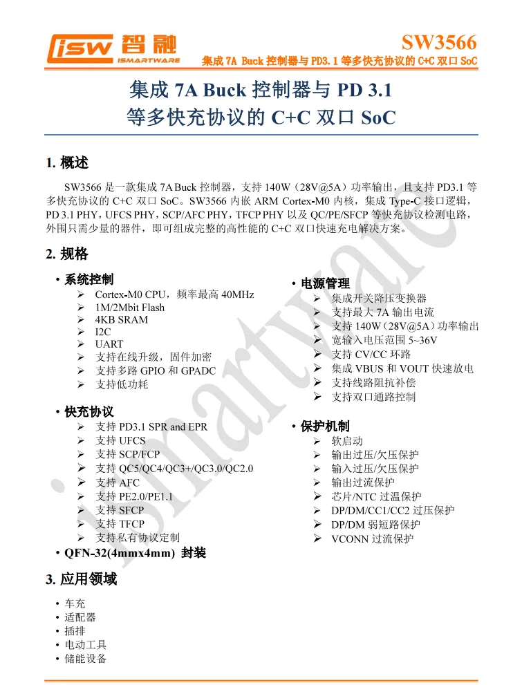
The SW3566H integrates CC/CV mode, dual-port management logic and bus voltage detection. When paired with the corresponding step-down switch tube and VBUS switch tube, it can achieve dual-port step-down output. The built-in step-down converter of the chip operates at a frequency of 180KHz and supports both PWM and PFM working modes. The protection thresholds such as output current and line loss compensation can all be set through the I2C interface. The built-in ADC can achieve data sampling of 9 channels including input and output voltage, output current, and chip temperature, and supports external MCU for parameter display.
The SW3566H supports an input voltage of 36V and a maximum output current of 7A. The chip is equipped with built-in soft start, input overvoltage/undervoltage protection, output overvoltage/undervoltage protection, output overcurrent/short circuit protection, DP/DM/CC overvoltage protection, chip overheat protection, external NTC thermistor protection, and power limiting protection. The chip is packaged in QFN4*4-32.
Charging Head Network Disassembly and understanding: Previously, Zhirong SW3566H was also equipped with Anker 65W 2C1A gallium nitride charger, Bull 240W 3C1A gallium nitride desktop charger, UGREEN 300W 4C1A five-port PD gallium nitride fast charging charger, Jinxiang 140W 3C1A gallium nitride fast charging charger, Gushi 188W multi-port desktop charger, and TOMAX 140W Topma Products such as 3C1A gallium nitride chargers have been adopted, and the performance and quality of the chips have been unanimously recognized by customers.
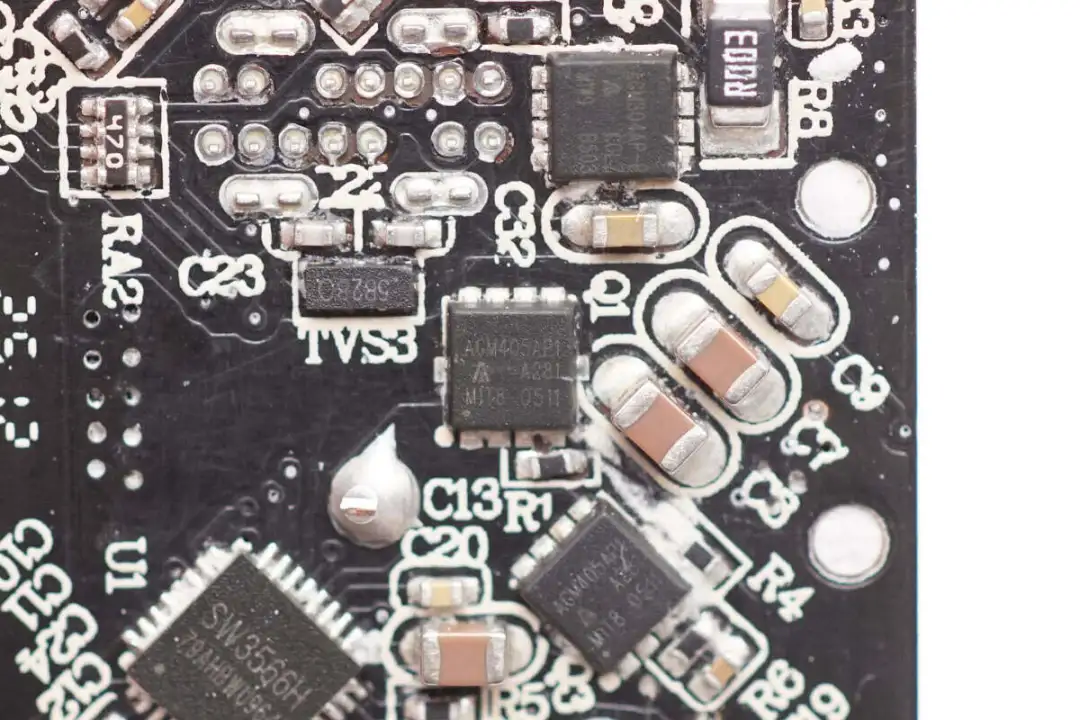
The synchronous step-down switch tube is from the core-controlled source, model AGM405AP1, NMOS, with a withstand voltage of 40V and a resistance of 5.7mΩ. It is packaged in PDFN3.3*3.3.
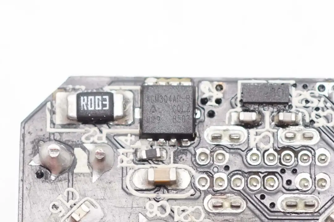
The VBUS switch tube is from the core-controlled source, model AGM304AP-B, NMOS, with a withstand voltage of 35V and a conductance of 3.1mΩ. It is packaged in PDFN3.3*3.3.
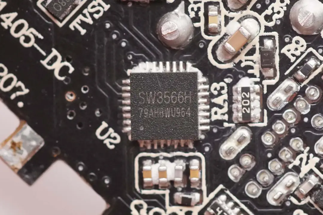
The USB-C2 interface adopts the SW3566H step-down protocol chip from Zhirong Technology.
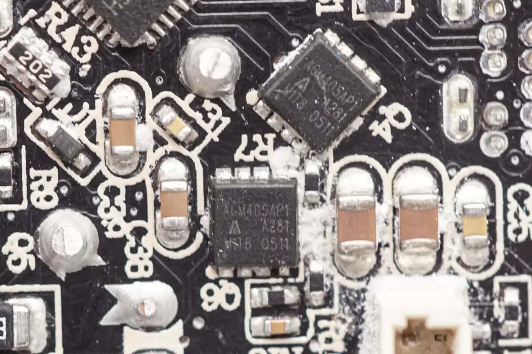
The synchronous step-down switch tube adopts the core-controlled source AGM405AP1.
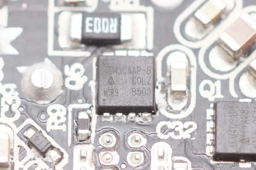
The VBUS switch tube adopts the core-controlled source AGM304AP-B.
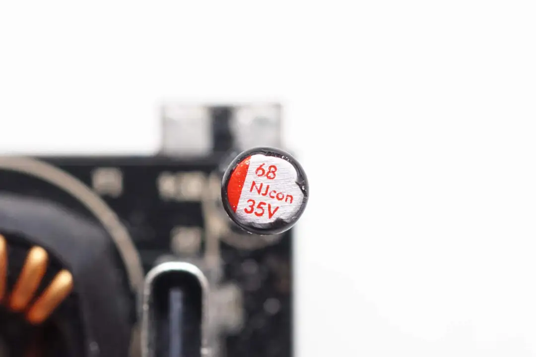
The input filter capacitor is from Yongli, with a specification of 68μF35V.
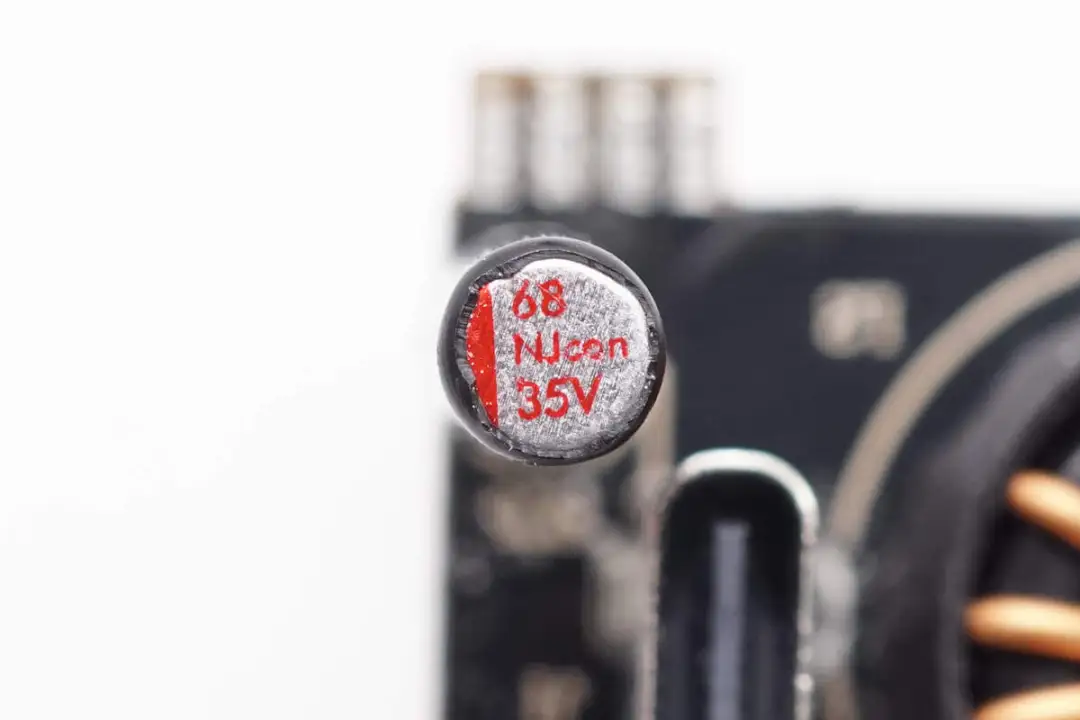
The other filter capacitor has the same specification.
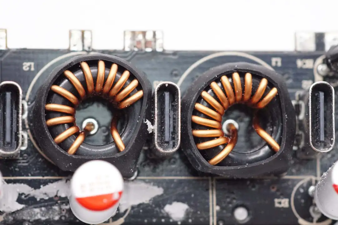
Close-up of two magnetic ring step-down inductors, insulated by heat shrink tubing on the outer jacket.
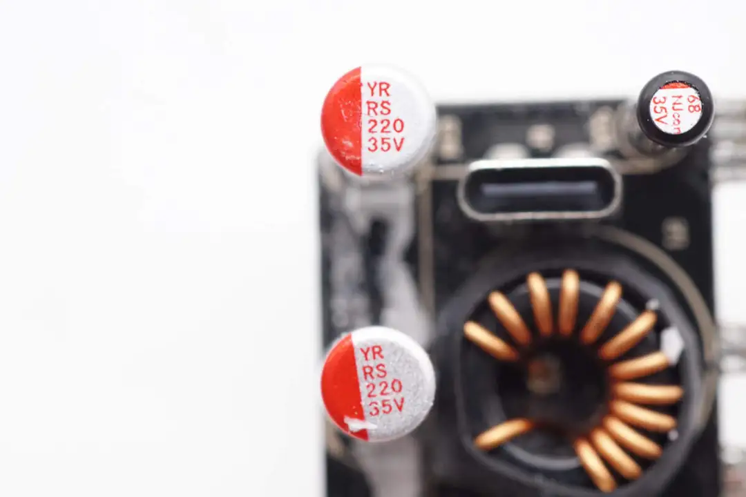
The specifications of the two filter capacitors are 220μF and 35V.
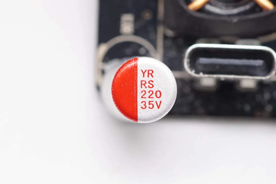
The third filter capacitor has the same specification.
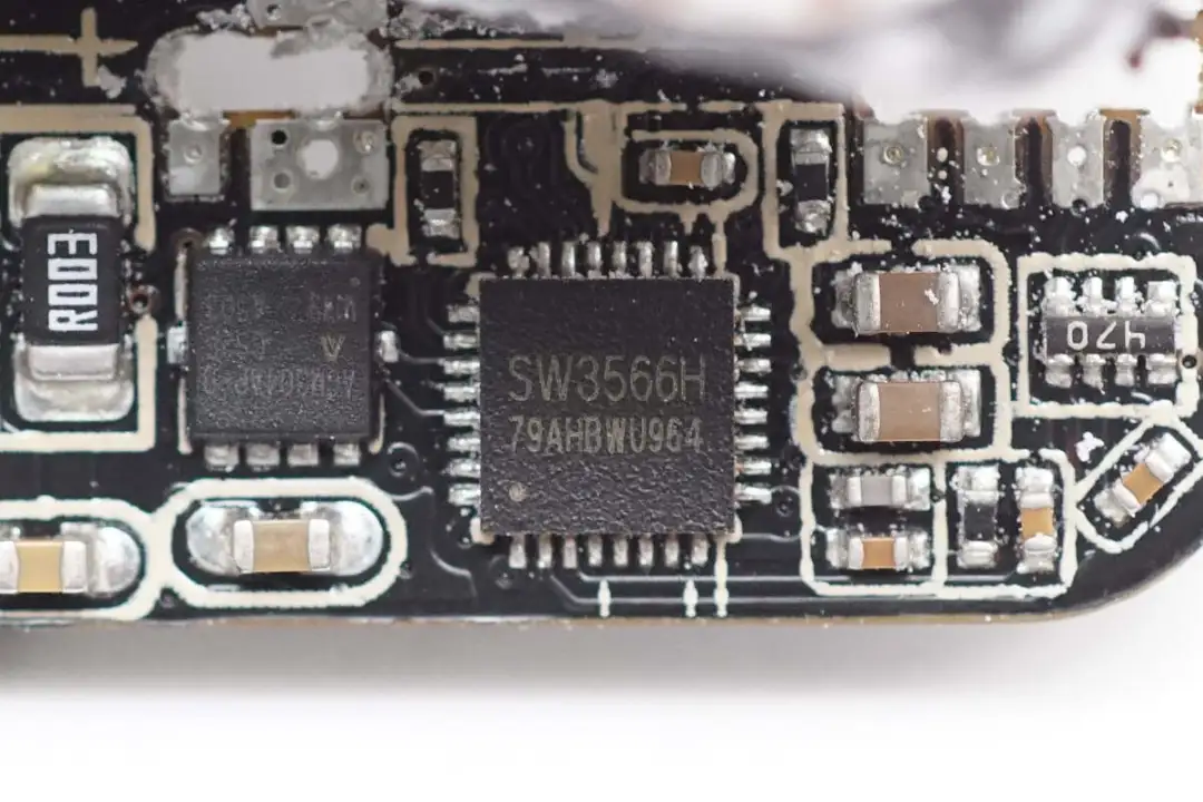
The USB-C3 interface also adopts the SW3566H step-down protocol chip from Zhirong Technology.
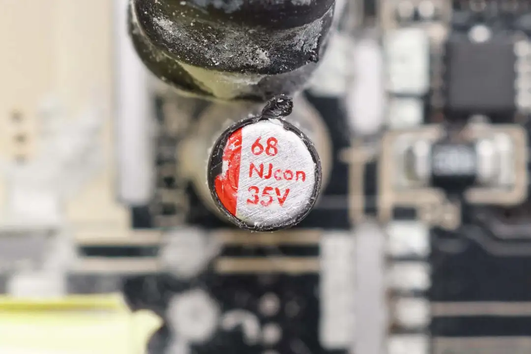
The specification of the input filter capacitor is 68μF35V.
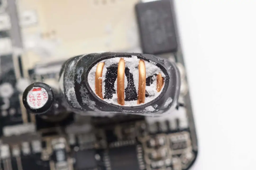
The magnetic ring step-down inductor is insulated by a heat shrink tube.
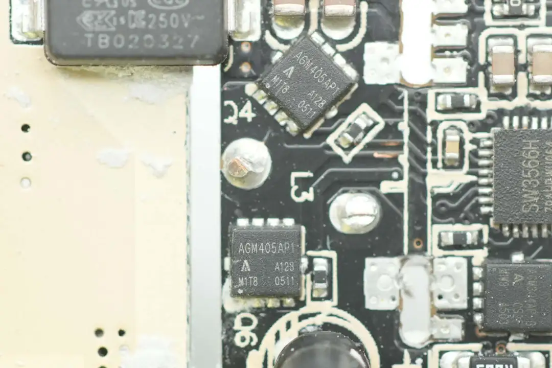
Under the step-down inductor, there is a synchronous step-down switch tube, which adopts the core-controlled source AGM405AP1.
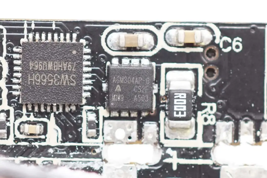
The VBUS switch tube adopts the core-controlled source AGM304AP-B.
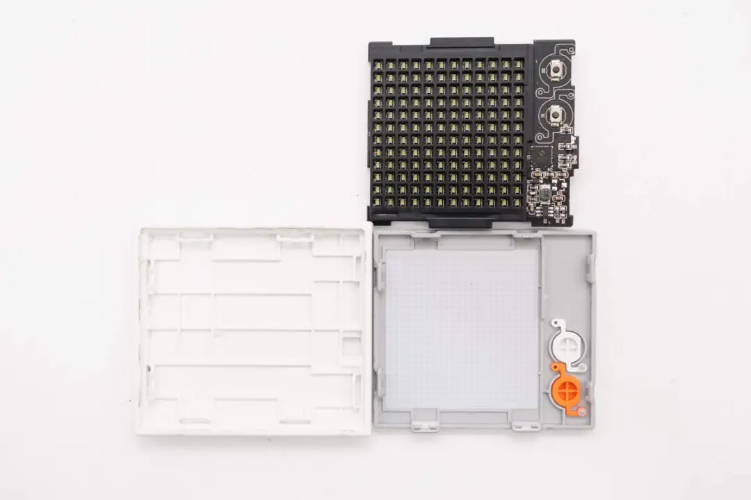
Finally, disassemble the dot matrix screen module. Remove the shell along the seams of the shell, and inside is the PCBA module.
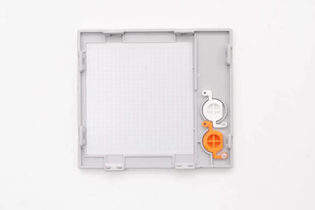
The grey cover plate is equipped with a smoothing plate and buttons inside.
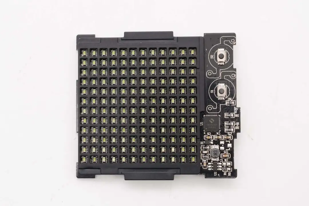
The front of the PCBA module is equipped with a surface mount LED dot matrix, and on the right side, there are surface mount buttons and a main control MCU.
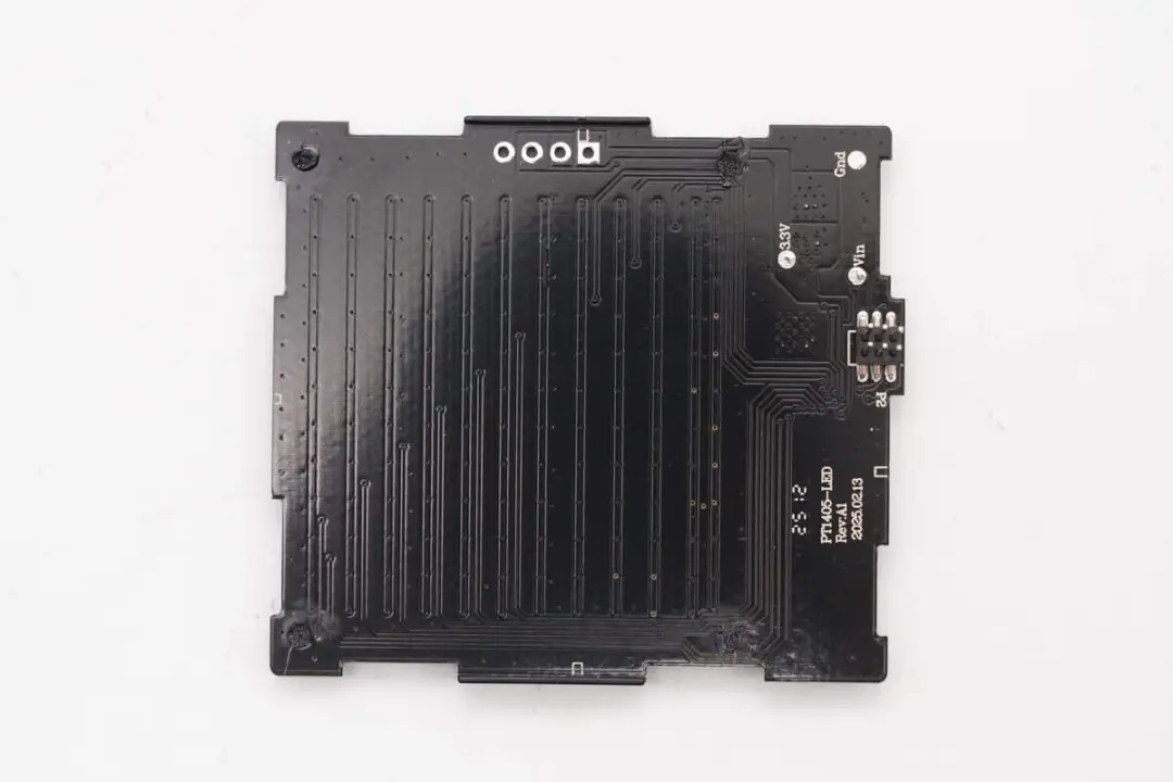
The back of the PCBA module features LED light traces.
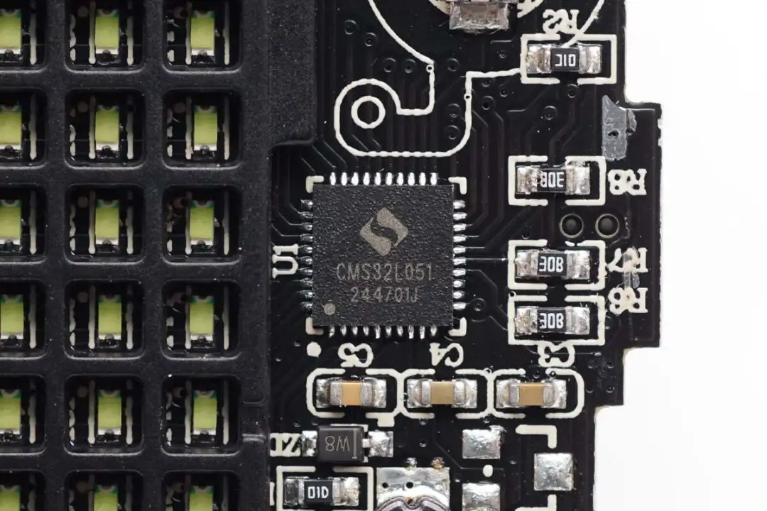
The MCU used for LED dot matrix screen control is from AMEC Semiconductor, model CMS32L051. The chip is equipped with an ARM Cortex-M0+CPU, 64KB SHARGE and 8KB SRAM, and is packaged in QFN40.
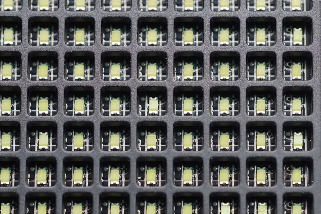
Close-up of the surface mount LED light, with plastic grilles for shading.
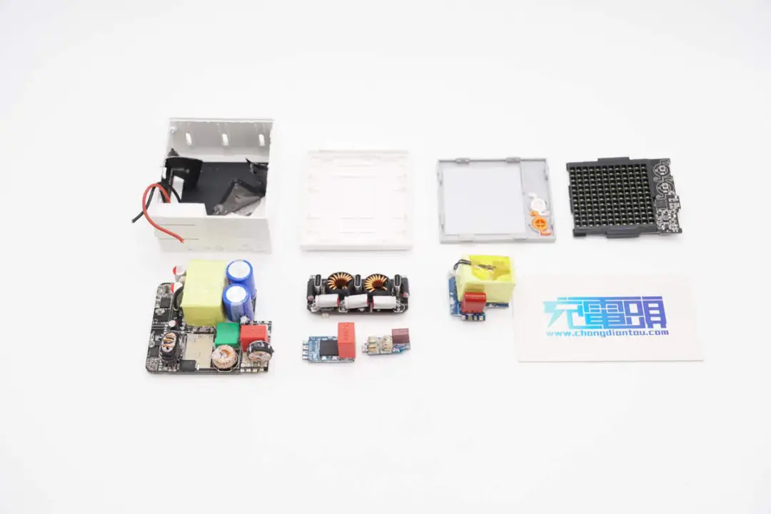
Take a complete disassembly and a family photo.
Charging Head Network Disassembly summary
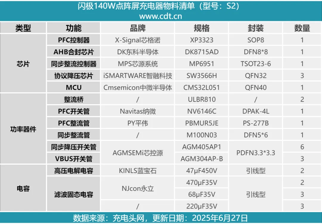
Finally, here is the list of core components of the SHARGE 140W dot matrix screen charger for your reference.
The SHARGE Dot Matrix Screen 140W gallium nitride charger adopts a square appearance design and is equipped with folding pins, making it convenient for daily carrying. The charger is equipped with three USB-C interfaces, supporting blind power insertion. When the interfaces are used simultaneously, automatic power allocation is supported. The digital display screen on the side of the body supports total output power display, individual interface power display, and supports brightness adjustment and Angle adjustment, which conforms to usage habits.
Charging Head Network learned through disassembly that this gallium nitride charger from SHARGE is composed of multiple PCBS welded together, making full use of space. The interior of the charger adopts a PFC+AHB architecture, using the XP3323 PFC controller from Xinggeno and the NV6146C gallium nitride switch tube from Navitas. The AHB encapsulation chip uses the DK8715AD from Dongke.
The charger is for step-down output. Three SW3566H chips from Zhirong Technology are used for the interface step-down output, and a core-controlled source switch tube is used in combination. The charger is equipped with an NTC thermistor for overheat protection. The output uses solid-state capacitors for filtering. The USB-C interface is provided with a TVS for electrostatic protection. The PCBA module is fully encapsulated with glue. Graphite stickers are pasted inside the shell for heat dissipation. The workmanship and materials are solid and reliable.
Source of the article: Charging Head Network